Method and apparatus for flat patterned media inspection

a flat patterned media and inspection method technology, applied in optical apparatus testing, structural/machine measurement, instruments, etc., can solve the problems of direct impact on inspection speed and system cost, over etching and under etching, and introduction of various production defects, so as to reduce the need for human intervention, increase the cycle time efficiency of the overall scheme, and minimize the effect of human intervention

Active Publication Date: 2008-06-10
ORBOTECH LTD
View PDF11 Cites 13 Cited by
  • Summary
  • Abstract
  • Description
  • Claims
  • Application Information

AI Technical Summary

Benefits of technology

[0024]By means of overlapping the low resolution defect detection and high resolution defect review and classification functionality, the present invention seeks to significantly reduce overall cycle time for the automatic optical inspection of flat, large, patterned articles. Applied to the TFT LCD inspection problem considered, this increases the value of the (Automated Optical Inspection Instrument) AOI instrument for the users which are usually operating under tight cycle-time constraints hence increase the chance of an AOI system being used for in-line 100% TFT-LCD plate inspection.
[0025]The inspection is facilitated through mechanical motion of the DRS imaging channels coordinated dynamically by means of a dispatching algorithm. This algorithm seeks to optimize the defect review effort by maximizing the number of high priority defect candidates captured by the DRS while minimizing the distance traveled by the sub-system modules. The inputs to this algorithm are the spatial distribution of the defect candidates detected by the DDS in the plane of the glass plate and the review worthiness factors assigned to the defect candidates by the DDS. The result of the dispatching algorithm is the optimal motion pattern for each individual DRS module. This motion pattern is then executed by the DRS motion system.
[0026]The optimal dispatching algorithm hence minimizes the number of defect candidates which cannot be reviewed with high resolution imaging of the DRS with a given number of camera modules. It also enables the priority capture of those defect candidates which are more important for high resolution imaging. Overall, this either results in the minimization of the number of camera modules required for a given defect candidate distribution, potentially reducing the system cost figure, or it improves the performance of the system with the same number of camera modules.
[0028]On-the-fly (OTF) focusing is typically a required feature of the present invention to realize the overlapped concurrent DDS / DRS system with low and high resolution by bringing the high resolution imaging system into sharp focus at the candidate defect locations. It increases the time efficiency of the overall scheme and enables the DRS to operate without stopping along the y-axis.
[0029]The real-time concurrent review and classification which is a part of the DRS minimizes the need for human intervention in the inspection process and increases the cycle time efficiency of the system.

Problems solved by technology

During each of the process stages and at various steps within a stage, various production defects may be introduced that affect the structure and that have electronic and / or visual implications on the final LCD panel product.
Such defects include but are not limited to circuit shorts, opens, foreign particles, mask problems, feature size problems, over etching and under etching.
The operating resolution of the system for automatic defect detection often has a direct impact on the inspection speed and the cost of the system.
Therefore, only comparatively lower resolutions are feasible to scan the entire area of the plate.
Unfortunately, at this lower resolution it has not been possible in the past to simultaneously perform both detection and reliable classification from the same image data collected.
Also, low resolution has an impact on the performance of the detection algorithms, which often result in a substantial number of false alarms which need to be eliminated.
If the minimum error over these combinations exceeds a threshold value, a defect is assumed.
Hence, they argue that the subsequent sub-pixel interpolation step would do little to improve the detected minimum and a false alignment would result, leading to false alarms in detection.
With any of the above methods, the use of a single feasible (comparatively low) resolution for scanning the entire surface of the article inspected leads to a set of defect candidates.
These defect candidates necessarily include both legitimate defects as well as false alarms, due to the inability of the methods to completely filter out expected variations between a test and reference image.
(a) Increased cycle time: The high resolution imaging stage comes immediately after the main detection stage. The sequential nature of the high resolution imaging has considerable impact on the inspection cycle time since the time required for high resolution image acquisition, review and classification is added to the time required for the detection scan.
(b) Idle imaging resources: The high resolution defect review imager is idle while the detection imager is active and the detection imager is idle while the review imager is active. This leads to an inefficient use of the system resources within the given time constraints.
(c) Non-optimal review process: When classification is necessary, and production environment time constraints prevent the imaging of all candidate locations, the user of the system may be left with the difficult task of deciding how many and which of the candidates to collect and process with the high resolution review imager.

Method used


Image

  • Method and apparatus for flat patterned media inspection
  • Method and apparatus for flat patterned media inspection
  • Method and apparatus for flat patterned media inspection

Examples


Embodiment Construction

[0037]Referring to FIG. 1, there is an illustration of some of the possible defects that can be found during the manufacturing process for LCD panels. These include a metal protrusion 110 into an ITO layer 112, an ITO protrusion 114 into metal 116, a so-called mouse bite crack 118 in metal 112, an open circuit 120 in metal 116, a transistor short 124 in the transistor 122 of a pixel, and a foreign particle 126 in any region. Each of these types of defects must be detected, classified and if possible repaired.

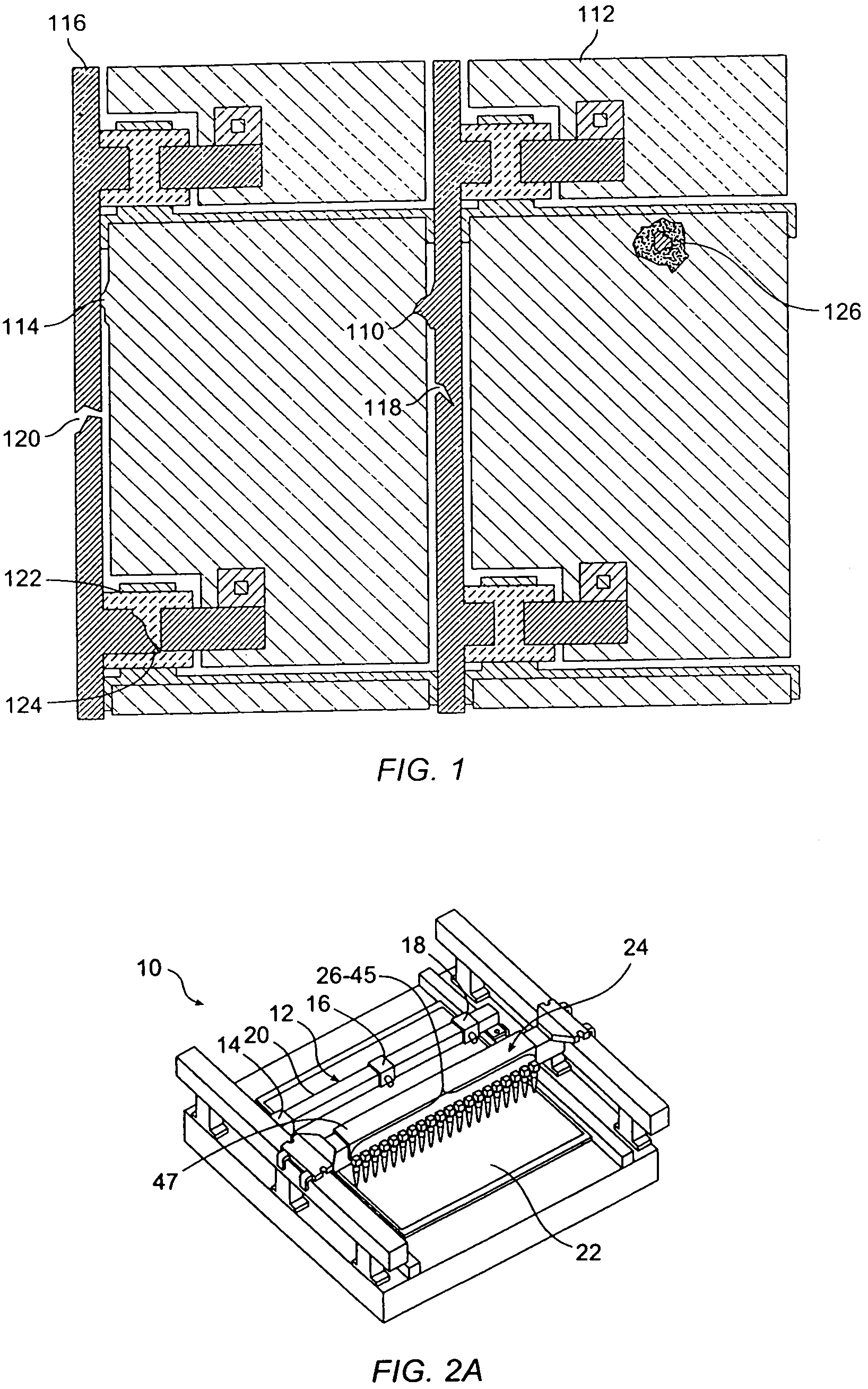
[0038]According to the invention, an inspection platform 10 (FIG. 2A or 2B) is provided with a Defect Review Sub-System (DRS) 12 which comprises a plurality of substantially identical, comparatively higher resolution imaging optics and optical-to-electrical converters together forming a set of camera modules 14, 16, 18 that are capable of moving together, as on a gantry 20 along the length of the article to be inspected 22 in coordination with scanning motion of a Defect Detecti...


PUM

PropertyMeasurementUnit
defectaaaaaaaaaa
dynamic defect reviewaaaaaaaaaa
distanceaaaaaaaaaa

Abstract

A concurrent low resolution / high resolution parallel scanning system and method are provided as an improvement in the scanning process of an inspection system for planar objects, such as large flat plates employed in panel displays, whereby lower resolution defect detection efficiently overlaps and parallels higher resolution defect review and classification stages in which defects are automatically defined and resolved. Although the invention is a valid solution for the more general problem of optically inspecting the surface of a flat article for defects, the invention is particularly useful for detecting pattern defects on large glass plates deposited with integrated-circuits for forming LCD flat panel displays.

Description

CROSS-REFERENCES TO RELATED APPLICATIONS[0001]The present application is a continuation of U.S. patent application Ser. No. 10 / 439,991 filed May 16, 2003 which claims benefit of the filing date of U.S. provisional application No. 60 / 423,008 filed on Nov. 1, 2002, the entire content of which is incorporated herein by reference.STATEMENT AS TO RIGHTS TO INVENTIONS MADE UNDER FEDERALLY SPONSORED RESEARCH AND DEVELOPMENT[0002]NOT APPLICABLEREFERENCE TO A “SEQUENCE LISTING,” A TABLE, OR A COMPUTER PROGRAM LISTING APPENDIX SUBMITTED ON A COMPACT DISK.[0003]NOT APPLICABLEBACKGROUND OF THE INVENTION[0004]The invention relates to the general field of machine vision based inspection technology and more particularly to machine vision based detection and classification of defects occurring on large flat patterned surfaces. In particular, the invention addresses the inspection of materials deposited on large substrate glass plates such as Liquid Crystal Display (LCD) panels. Although the inventi...

Claims


Application Information

Patent Timeline
Patent Type & Authority Patents(United States)
IPC IPC(8): G06K9/00G01M11/00G01B11/30G01N21/956G02F1/13G06T1/00G06T7/00
CPCG01N21/95607G06T7/001G01N2021/9513G02F1/13
Inventor WEISS, ADAMSARANLI, AFSAR
Owner ORBOTECH LTD
Why Eureka
Try Eureka