Thin film piezoelectric resonator, thin film piezoelectric device, and manufacturing method thereof

a piezoelectric device and thin film technology, applied in piezoelectric/electrostrictive/magnetostrictive devices, piezoelectric/electrostriction/magnetostriction machines, impedence networks, etc., can solve the problems of large insertion loss of thin film piezoelectric devices prepared by combining a plurality of fbar resonators, long complicated steps are required, and the planar shape of the diaphragm is preferably

Active Publication Date: 2008-06-17
MEMS SOLUTIONS INC
View PDF19 Cites 56 Cited by
  • Summary
  • Abstract
  • Description
  • Claims
  • Application Information

AI Technical Summary

Benefits of technology

[0015]The present invention has been developed in consideration of the above-described problems, and an object of the present invention is to provide a thin film piezoelectric device which is prepared by combining a plurality of resonators constituted of an FBAR or an SBAR having a large electromechanical coupling coefficient and superior acoustic quality factor (Q value) and frequency temperature characteristic and whose insertion loss is small and whose performance has been improved.
[0016]According to the present invention, to achieve the above-described object, there are provided the following high-performance thin film piezoelectric device which is superior in the acoustic quality factor, bandwidth, temperature characteristic and the like and whose insertion loss is small, and a method of manufacturing the device.
[0017]It has been known that the insertion loss of the thin film piezoelectric device, for example, a filter prepared by combining a plurality of thin film piezoelectric resonators depends on a conductor loss of a metal electrode layer. The present inventors have considered that electric resistance of a metal electrode electrically connected to adjacent thin film piezoelectric resonators drops, when a distance between centers of the adjacent thin film piezoelectric resonators is shortened, and, as a result, the insertion loss can be largely lowered. Then, as a result of various studies of measures to shorten the distance between the centers of the adjacent thin film piezoelectric resonators, it has been found that applying of anisotropic etching by a deep graving type reactive ion etching (deep RIE) process which is deep trench etching utilizing plasma is most preferable solving means both in improvement of the performance of the thin film piezoelectric device and reduction of the cost.

Problems solved by technology

An SAW filter has met user's strictly required specifications by improvement of design and production technique, but improvement of characteristics has been nearly limited with increase of a utilized frequency, and a great technical innovation has been required both in miniaturization of electrode formation and securement of stable output.
Therefore, there is a problem that insertion loss of the thin film piezoelectric device prepared by combining a plurality of FBAR resonators becomes remarkably large.
However, in this method, a long complicated step is required.
As the manufacturing step is long and complicated, the cost of the device is increased, yield of a product drops, which results in further increase of the cost of the device.
It is difficult to spread this expensive device as a general-purpose component for a mobile communication apparatus.
Since the liquid etching reagent for use in removing sacrificial materials such as phosphor silicate glass (PSG) corrodes the layers of the lower electrode, the piezoelectric thin film, and the upper electrode constituting the upper structure, the materials usable in the upper structure are remarkably limited, Furthermore, there is a serious problem that it is difficult to prepare an FBAR or SBAR structure having a desired dimensional precision.
For example, when the electrode layer or the substrate film is thickened, there is a problem that effective electromechanical coupling coefficient of the FBAR or SBAR is reduced.
On the other hand, when the metal electrode layer is thinned and elongated, conductor loss becomes higher by the increase of electric resistance, and therefore various restrictions are generated in designing the structure of the thin film piezo electric device prepared by combining a plurality of FBARs or SBARs.
The thin film piezoelectric device exerting a sufficient performance in a gigahertz band has not been obtained for the above reason.

Method used


Image

  • Thin film piezoelectric resonator, thin film piezoelectric device, and manufacturing method thereof
  • Thin film piezoelectric resonator, thin film piezoelectric device, and manufacturing method thereof
  • Thin film piezoelectric resonator, thin film piezoelectric device, and manufacturing method thereof

Examples


example 1

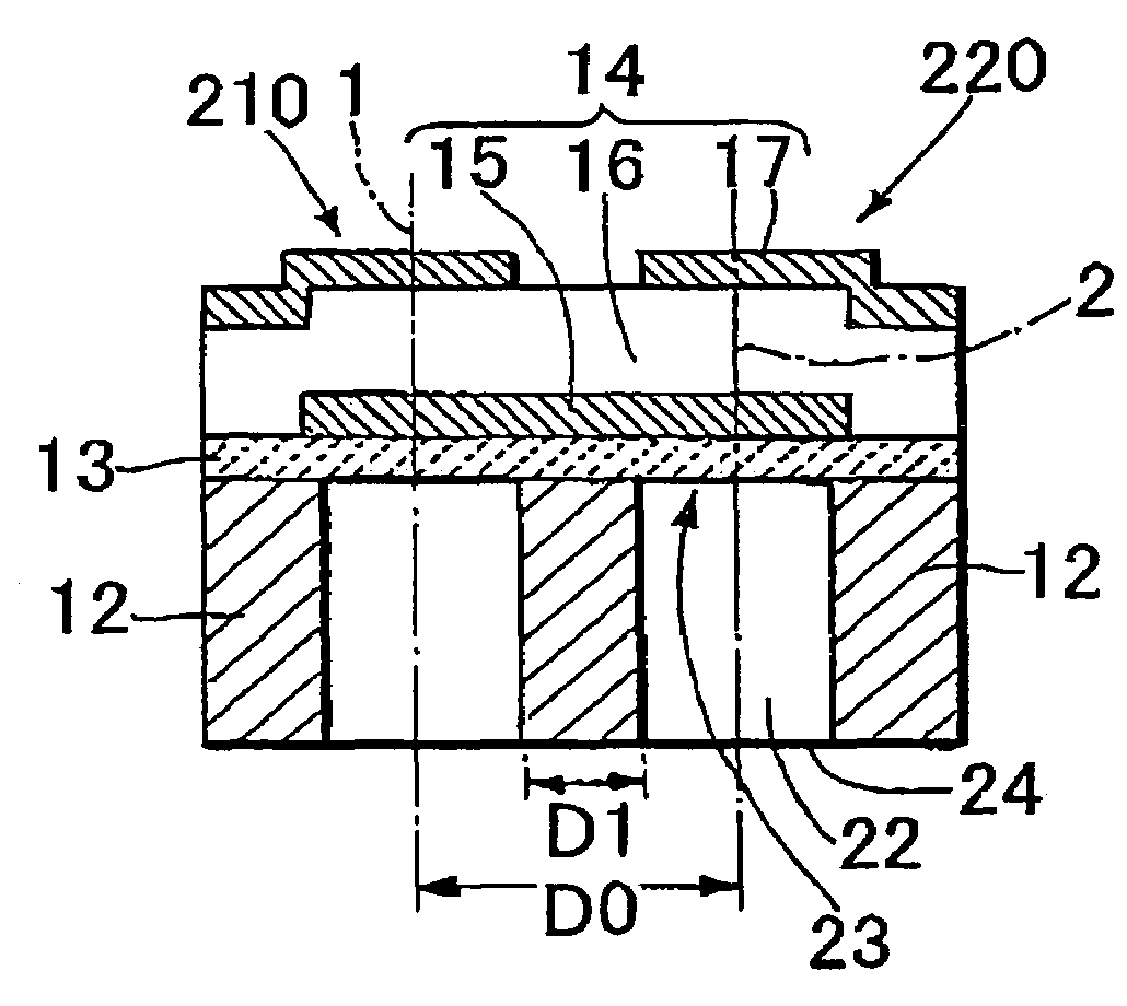
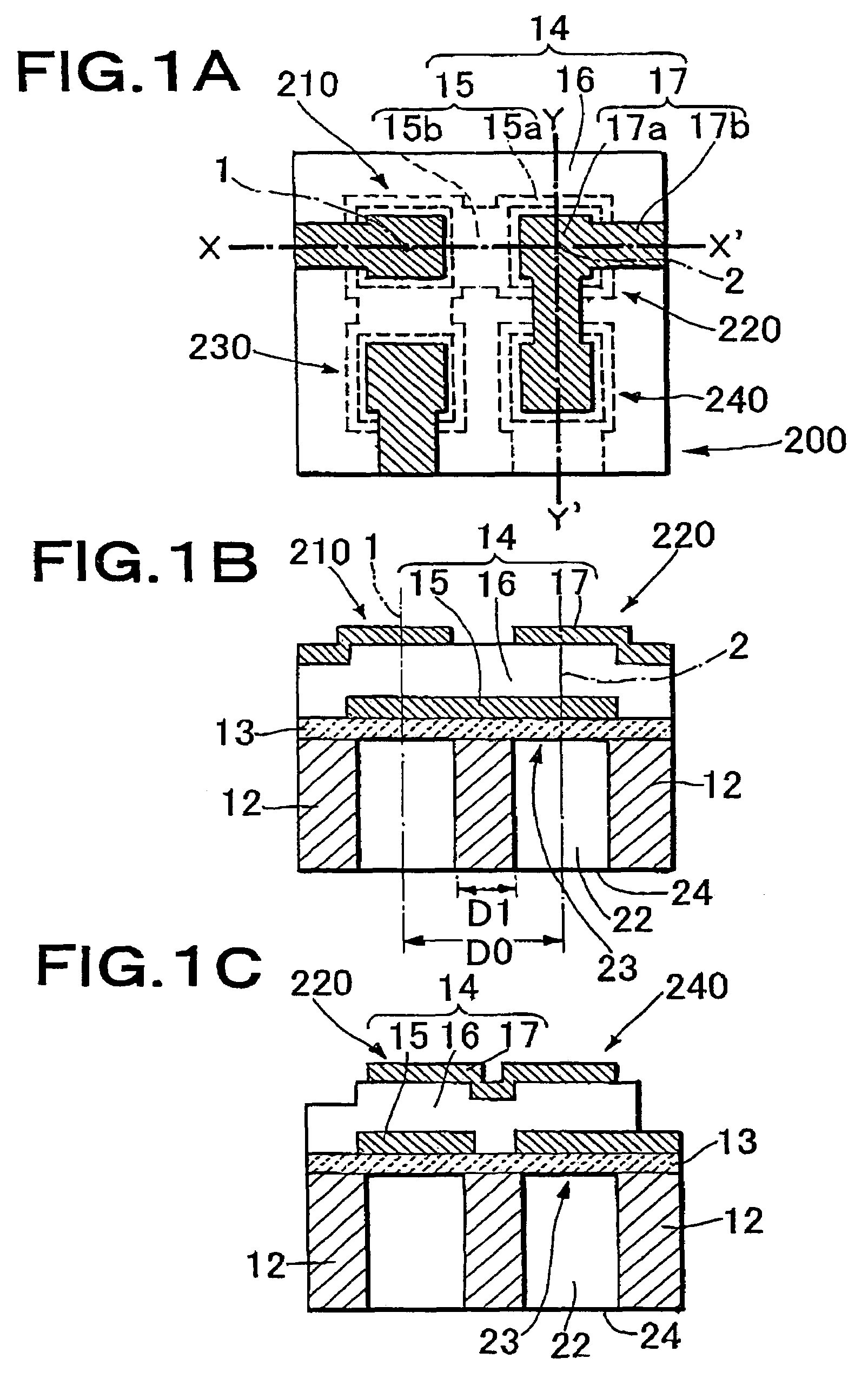
[0112]In the present example, a thin film piezoelectric filter shown in FIGS. 2A to 2C was prepared as follows.

[0113]That is, the upper surface of a (100) Si substrate 12 having a thickness of 250 μm was patterned and etched into a desired shape by photolithography, so that a depression was disposed in periphery thereof in such a manner that a flat base having a nearly rectangular shape with a height of 3.0 μm and a planar dimension of about 140×160 μm was left. It is to be noted that the base was formed in a position corresponding to a diaphragm of an resonator to be formed. After forming SiO2 layers each having a thickness of 1.0 μm on opposite upper / lower surfaces of a substrate by a thermal oxidation method, an SiO2 layer having a thickness of 3.5 μm was deposited on the upper surface of the substrate at 450° C. by a thermal CVD method using tetraethoxy silane (Si(O(C2H5)4) in a raw material, and annealed at 1000° C. Next, the SiO2 layer on the upper surface of the substrate was...

example 2

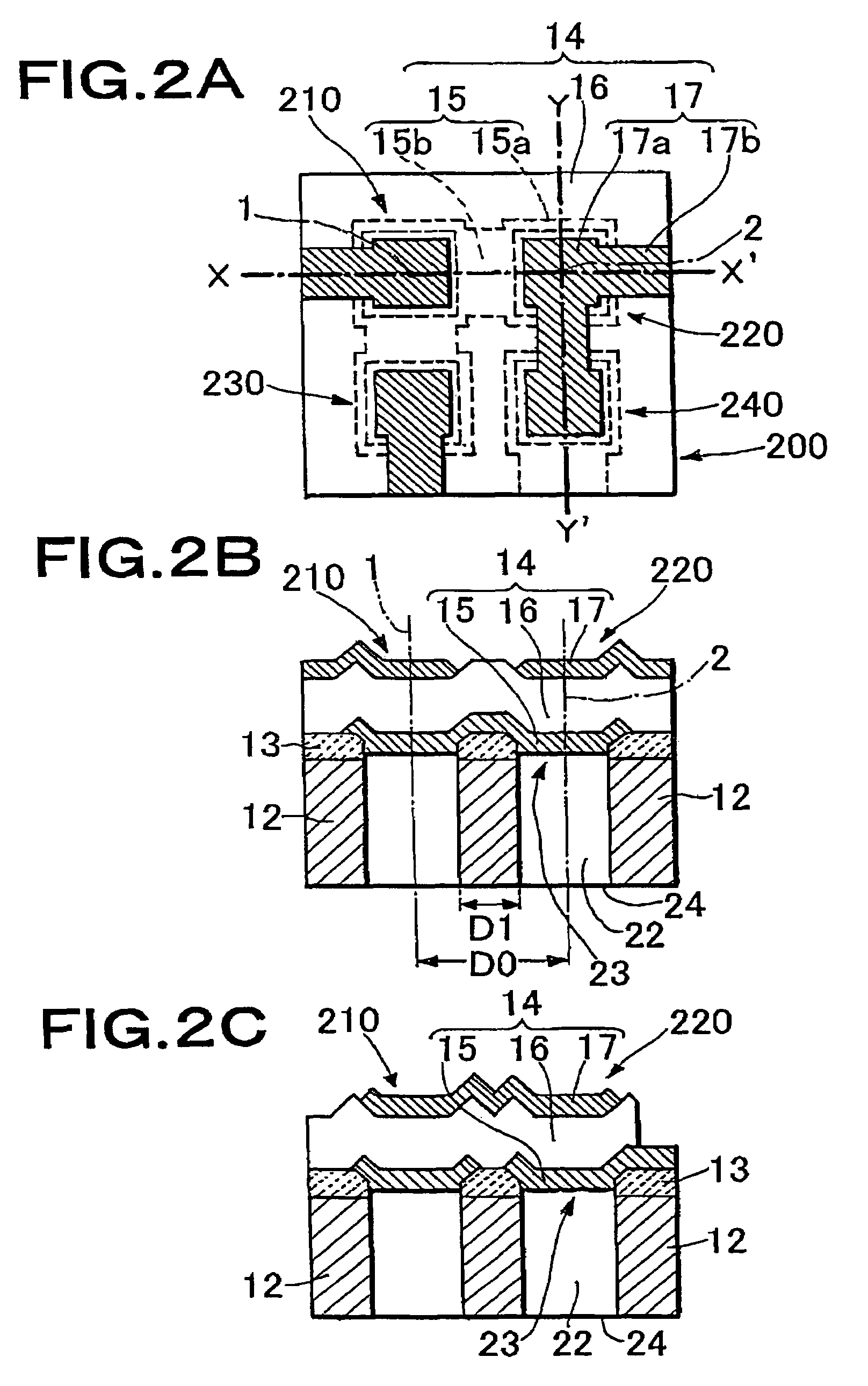
[0124]In the present example, a thin film piezoelectric filter having the structure (the diaphragm 23 is trapezoidal) shown in FIG. 2 was prepared as follows.

[0125]That is, an procedure similar to that of Example 1 was repeated to prepare the thin film piezoelectric filter comprising the ladder type circuit except that a Ti metal layer (adhesive layer), a Pt metal layer (intermediate layer), and a Mo metal layer (main electrode layer) were deposited as a lower electrode in this order to form a Mo / Pt / Ti lower electrode 15 having a material and thickness described in Table 1, a Ti metal layer (adhesive layer) and a Mo metal layer (main electrode layer) were deposited as an upper electrode in this order to form a Mo / Ti upper electrode 17 having a material and thickness described in Table 1, and the planar shape of a via hole fabricated by deep RIE was formed to be trapezoidal to thereby form a diaphragm 23 into a trapezoidal shape. The above described D1 / D0 of the present example was 0...

example 3

[0129]In the present example, a thin film piezoelectric filter having the structure (the diaphragm 23 was trapezoidal) shown in FIG. 1 was prepared as follows.

[0130]That is, after forming SiO2 layers each having a thickness of 1.2 μm on opposite upper / lower surfaces of a (100) Si substrate 12 having a thickness of 250 μm by a thermal oxidation method, the only SiO2 layer on the upper surface was etched to adjust the thickness of the SiO2 layer on the upper surface, and an insulating layer 13 made of SiO2 and having a thickness value described in Table 1 was formed. A Ti metal layer (adhesive layer), an Au metal layer (intermediate layer), and a Mo metal layer (main electrode layer) were deposited on the upper surface of the insulating layer 13 in this order by a DC magnetron sputtering method, and patterned into a desired shape by photolithography to form a Mo / Au / Ti lower electrode 15. A main body portion 15a of the lower electrode 15 was formed into a nearly rectangular shape. It w...


PUM


Abstract

A thin film piezoelectric device includes a substrate (12) having via holes (22) and a piezoelectric laminated structure (14) consisting of a lower electrode (15), a piezoelectric film (16), and an upper electrode (17) formed on the substrate (12) via an insulation layer (13). A plurality of thin film piezoelectric resonators (210, 220) are formed for the via holes (22). The piezoelectric laminated structure (14) includes diaphragms (23) located to face the via holes (22) and a support area other than those. The thin film piezoelectric resonators (210, 220) are electrically connected by the lower electrode (15). When the straight line in the substrate plane passing through the centers (1, 2) of the diaphragms (23) of the thin film piezoelectric resonators (210, 220) has the length D1 of the segment passing through the support area and the distance between the centers of the diaphragms of the thin film piezoelectric resonators (210, 220) is D0,the ratio D1 / D0 is 0.1 to 0.5. The via hole (22) is fabricated by the deep graving type reactive ion etching method.

Description

[0001]This application is a 371 of PCT / JP2003 / 007857 filed on Jun. 20, 2003, published on Dec. 31, 2003 under publication number WO 2004 / 001964 A1 which claims priority benefits from Japanese Patent Application Number 2002-179910 filed Jun. 20, 2002.TECHNICAL FIELD[0002]The present invention relates to a thin film piezoelectric device prepared by combining a plurality of thin film piezoelectric resonators utilizing piezoelectric thin films and, in more detail, relates to a thin film piezoelectric resonator for use in a filter for a communication apparatus, a thin film piezoelectric device, and a method of manufacturing the device.[0003]Moreover, the present invention relates to a thin film piezoelectric resonator utilizing a piezoelectric thin film for use in broad fields such as a thin film filter for use in a mobile communication apparatus or the like, a duplexer or transmission / reception switching unit, a thin film voltage control oscillator (VCO), various types of sensors and th...

Claims


Application Information

Patent Timeline
Patent Type & Authority Patents(United States)
IPC IPC(8): H01L41/08H01L41/22H01L41/29H03H3/02H03H9/02H03H9/56H03H9/58
CPCH03H3/02H03H9/02094H03H9/02102H03H9/02157H03H9/562H03H9/564H03H9/568H03H9/585H03H9/588
Inventor YAMADA, TETSUONISHIMURA, KOSUKENAGAO, KEIGO
Owner MEMS SOLUTIONS INC
Why Eureka
Try Eureka