Solid-state image sensor and image reading method

a solid-state image sensor and reading method technology, applied in the field of solid-state image sensors and image reading methods, can solve the problems of low yield risk of image sensors with 3-tr-pixels, -state image sensors having 4-tr-pixels, and -state image sensors having 3-tr-pixels. junction leakage can be reduced, the electric field of pn junction of floating diffusion fd can be reduced, and the area increased

Inactive Publication Date: 2008-06-24
FUJITSU SEMICON LTD
View PDF12 Cites 29 Cited by
  • Summary
  • Abstract
  • Description
  • Claims
  • Application Information

AI Technical Summary

Benefits of technology

[0029]In the solid-state image sensor according to the present invention, any two of the gate electrode of the transfer transistor, the gate electrode of the reset transistor and the gate electrode of the select transistor are formed of one continuous pattern of the same conducting layer, whereby allowance can be given to layouts of the metal interconnection layers. Accordingly, the floating diffusions can be effectively shielded from light. Furthermore, allowance can be given to the area. Accordingly, the floating diffusions can have the area increased, so that the electric field of PN junction of the floating diffusion FD can be reduced without decreasing the floating diffusion FD capacitance, whereby the junction leakage can be redu

Problems solved by technology

It is said that the solid-state image sensors having 3-Tr-pixels are vulnerable to noises due to thermal noises (kTC noises).
The solid-state image sensor having 4-Tr-pixels, which has more constituent elements than the solid-state image sensor having 3-Tr-pixe

Method used


Image

  • Solid-state image sensor and image reading method
  • Solid-state image sensor and image reading method
  • Solid-state image sensor and image reading method

Examples


first embodiment

A First Embodiment

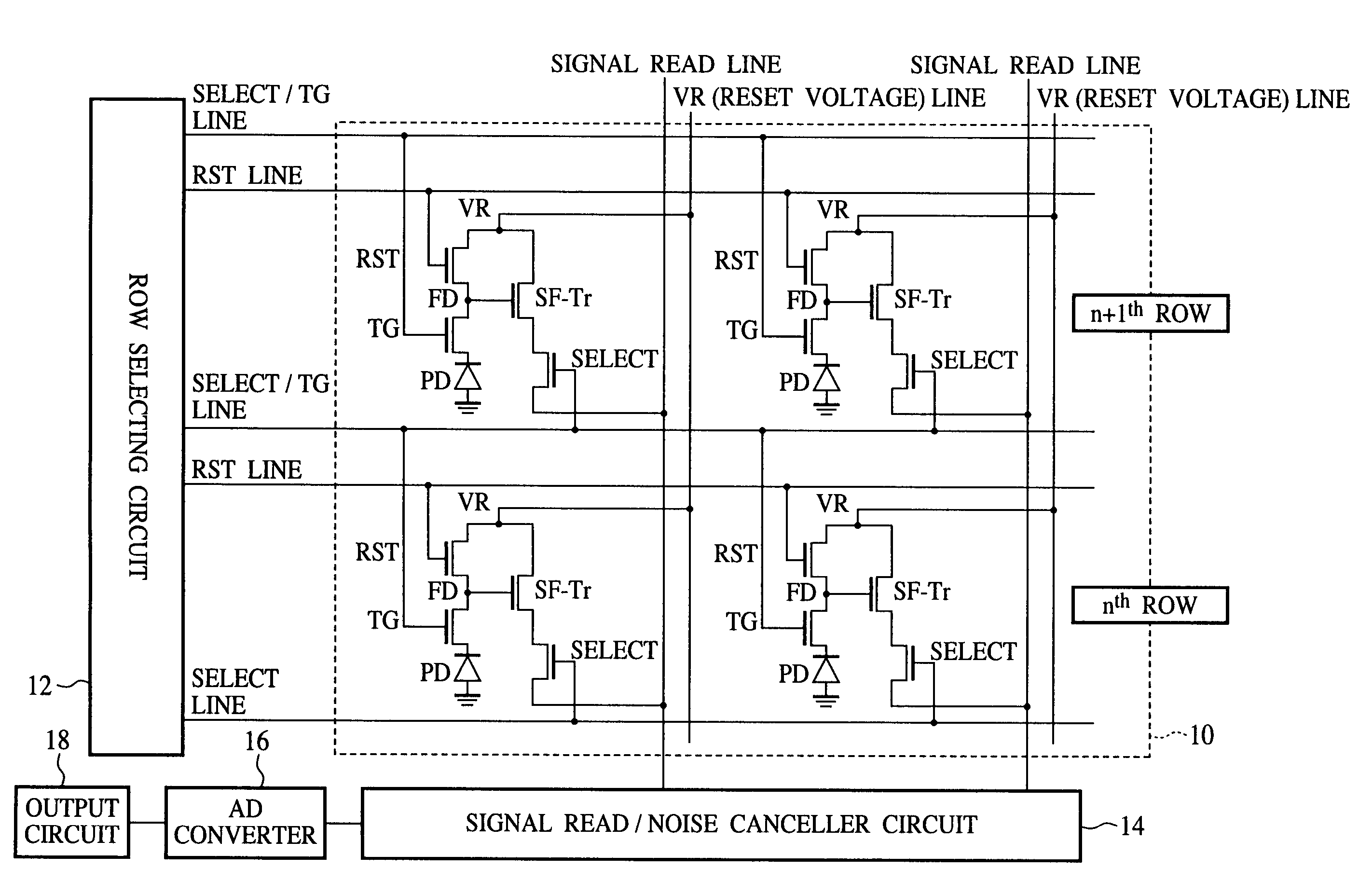
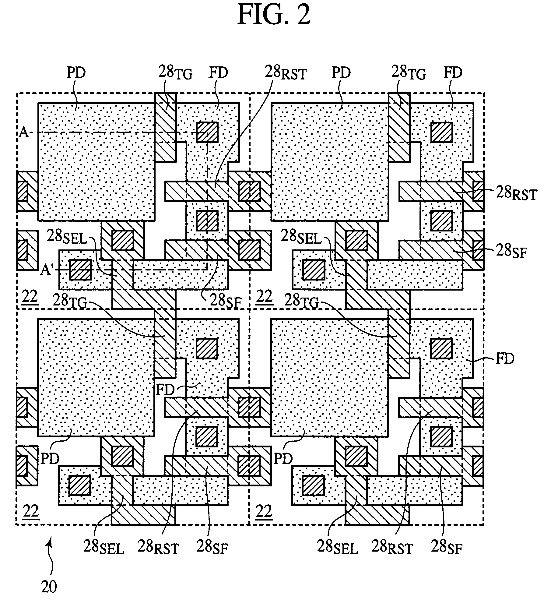
[0055]The solid-state image sensor according to a first embodiment of the present invention will be explained with reference to FIGS. 1 to 8.

[0056]FIG. 1 is a circuit diagram of the solid-state image sensor according to the present embodiment. FIGS. 2 to 5 are plan views of the solid-state image sensor according to the present embodiment, which show a structure thereof. FIGS. 6A and 6B are timing charts explaining the image reading method of the solid-state image sensor according to the present embodiment. FIGS. 7A-7C and 8 are sectional views of the solid-state image sensor according to the present embodiment in the steps of the method for fabricating the same, which show the method.

[0057]First, the structure of the solid-state image sensor according to the present embodiment will be explained with reference to FIGS. 1 to 5. FIG. 1 is a circuit diagram of the solid-state image sensor according to the present embodiment. In FIG. 1, a pixel array unit 10 is represen...

second embodiment

A Second Embodiment

[0117]The solid-state image sensor according to a second embodiment of the present invention will be explained with reference to FIGS. 9 to 12.

[0118]FIGS. 9 to 12 are plan views of the solid-state image sensor according to the present embodiment, which show a structure thereof. The same members of the present embodiment as those of the solid-state image sensor according to the first embodiment shown in FIGS. 1 to 8 are represented by the same reference numbers not to repeat or to simplify their explanation.

[0119]The solid-state image sensor according to the present embodiment is the same as the solid-state image sensor according to the first embodiment in the circuit diagram, the operation and the fabrication method except that the plane layouts of the respective layers are different from those of the solid-state image sensor according to the first embodiment. That is, in the solid-state image sensor according to the present embodiment as well, a TG line commonly ...

third embodiment

A Third Embodiment

[0130]The solid-state image sensor according to a third embodiment of the present invention will be explained with reference to FIGS. 13 to 16.

[0131]FIGS. 13 to 16 are plan views of the solid-state image sensor according to the present embodiment, which show a structure thereof. The same members of the present embodiment as those of the solid-state image sensor according to the first and the second embodiments are represented by the same reference numbers not to repeat or to simplify their explanation.

[0132]The solid-state image sensor according to the present embodiment is the same as the solid-state image sensor according to the first embodiment in the circuit diagram, the operation and the fabrication method except that the layouts of the respective layers are different from those of the first embodiment. That is, in the solid-state image sensor according to the present embodiment as well, a TG line commonly connecting the gate terminals of the transfer transist...


PUM


Abstract

In the solid-state image sensor comprising 4-Tr-pixels, TG lines connecting the gate electrodes 28TG of the transfer transistors of the pixel units of the nth row, and select lines connecting the gate electrodes 28SEL of the select transistors of the pixel units of the n+1th row are formed of a common signal line, and the gate electrodes 28TG of the pixels of the nth row and the gate electrodes 28SEL of the pixel units of the n+1th row are formed in one continuous pattern of the same conducting layer. Whereby allowance can be given to layouts of the metal interconnection layers. Accordingly, the floating diffusions FD can be effectively shielded from light. Furthermore, allowance can be given to the area. Accordingly, the floating diffusions FD can have the area increased, whereby the junction leakage can be reduced.

Description

CROSS-REFERENCE TO RELATED APPLICATIONS[0001]This application is based upon and claims the benefit of priority from the prior Japanese Patent Application No. 2002-257131, filed in Sep. 2, 2002, the entire contents of which are incorporated herein by reference.BACKGROUND OF THE INVENTION[0002]The present invention relates to a solid-state image sensor and an image reading method, more specifically a solid-state image sensor having 4-Tr-pixels and an image reading method for the solid-state image sensor.[0003]Solid-state image sensors basically formed of CMOS generally use the structure called APS (Active Pixel Sensor), which comprises photodiodes for converting optical signals to electric signals, reset transistors for resetting the photodiodes, source follower transistors for converting signal charges of the photodiodes to voltages to output the signal charges in voltage, and select transistors for connecting / selecting pixels and signal lines. Solid-state image sensors formed of the...

Claims


Application Information

Patent Timeline
IPC IPC(8): H04N3/14H01L27/00H04N5/335H01L31/062H01L27/146H04N5/369H04N5/374
CPCH01L27/14603H04N3/155H01L27/14643H01L27/14623H04N25/766H01L27/146
Inventor OHKAWA, NARUMI
Owner FUJITSU SEMICON LTD
Why Eureka
Try Eureka