Sensor device

a microanalysis system and sensor technology, applied in the field of microanalysis system sensor devices, can solve the problems of inapplicability, inability to generate fluorescence fluorescence, and inability to meet the requirements of the system, so as to achieve the effect of reducing the noise componen

Inactive Publication Date: 2008-06-24
CANON KK
View PDF4 Cites 14 Cited by
  • Summary
  • Abstract
  • Description
  • Claims
  • Application Information

AI Technical Summary

Benefits of technology

[0018]The sensor device of the present invention in which plural photonic crystal regions are optically connected enables decrease of a noise component caused by external disturbance.

Problems solved by technology

Further, cost-down of the system can be expected by the miniaturization.
In the fluorescence labeling method, a desirable label, namely a label sufficiently sensitive for the detection, is not necessarily applicable owing to compatibility between the objective substance and the labeling substance.
Further, in this method, the fluorescence as the signal component is interfered less by the intense exciting light as a noise because of the wavelength difference between the exciting light and the fluorescence advantageously, but the generation efficiency of the fluorescence as the signal component cannot readily be raised, which renders difficult to improve the total SN ratio.
On the other hand, in this method, when the concentration of the objective substance is lowered to solve the above disadvantage, the original signal becomes weak to lower the SN ratio, also.
Furthermore, even though the influence of the light is not remarkable, the light penetrating through the objective fluid may cause heat generation or a photoreaction, so that the intensity of the light should be limited.
However, the wavelength of the light for detection of a change or loss and the wavelength of the irradiated light are the same, which requires extremely large dynamic range of the detector, disadvantageously.
Therefore, with this measurement method, a slight loss by a slight degree of reaction in the micro flow channel cannot be measured with a high accuracy.
The constitution of small integration or a low cost cannot be equipped with such a temperature control means.
In such an operation sequence, fluctuation of the concentration, temperature, or density of the buffer solution directly causes fluctuation of the baseline to produce a noise component.
This causes a cost increase and a larger size of the device.

Method used


Image

  • Sensor device
  • Sensor device
  • Sensor device

Examples


example 1

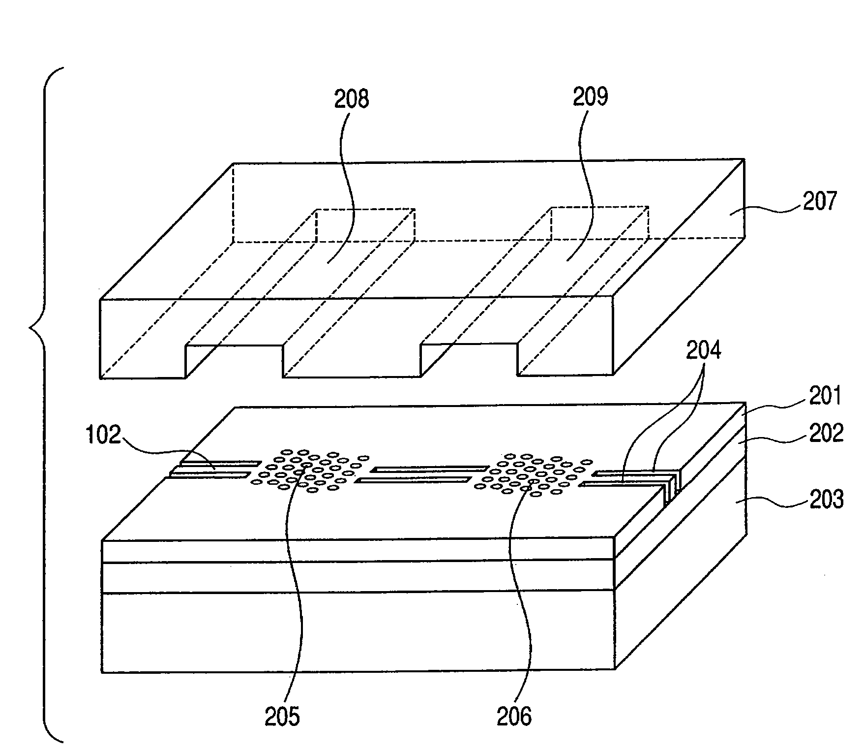
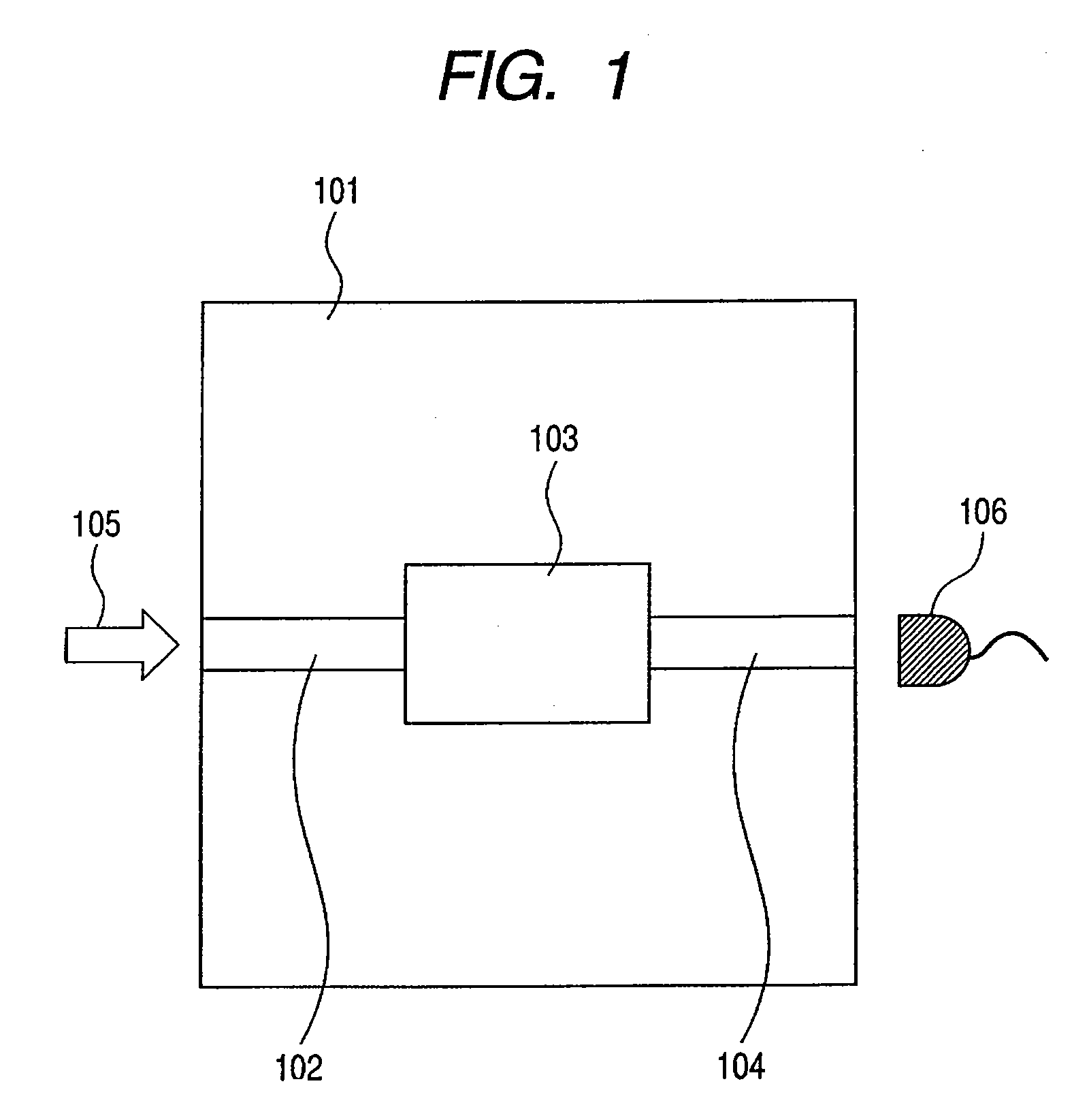
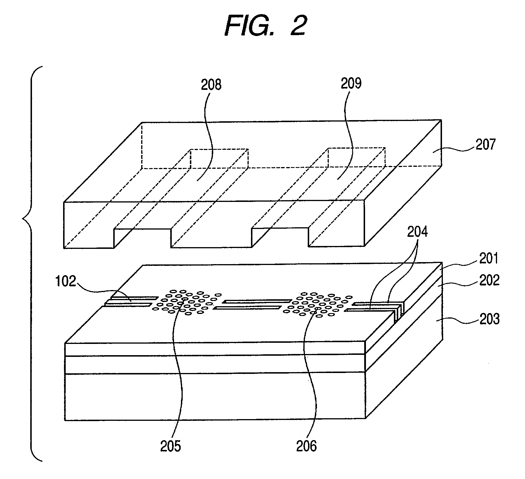
[0049]Two photonic crystals different in a property are optically connected serially, and sensing is conducted by utilizing transmitted light having transmitted through the two photonic crystals. The entire constitution of the sensor device of this Example is explained by reference to FIG. 1.

[0050]In FIG. 1, on substrate 101, photonic-crystal optical element system 103 is placed between light-introduction-side optical waveguide 102 and output-side optical waveguide 104. Incident light 105 is introduced from the outside of the element for measurement of the spectral transmittance of the photonic crystal optical element system. Optical detector device 106 detects the light having transmitted through optical waveguide 102, photonic crystal optical element system 103, and optical waveguide 104.

[0051]The photonic crystal optical element system in combination with a micro flow channel mentioned below will change its spectral transmissivity in accordance with an environmental change caused...

example 2

[0067]In this Example, two defect-containing photonic crystals having the same properties are optically connected in series, and sensing is conducted the utilizing transmitted light having transmitted through the two photonic crystals. The sensor device of this Example has a constitution similar to that shown in FIG. 1 as a whole. The photonic crystal element system is also similar to that in Example 1, and is shown in FIGS. 5A-5C. This example is different from Example 1 in first photonic crystal 205, second photonic crystal 206, and the incident light 105 for the detection.

[0068]In this Example, the two same photonic crystals are employed which have respectively a deficiency of a cylindrical hole and a defect-resonator 501. Thereby, the spectral transmittance of the photonic crystal has a sharp transmission peak corresponding to the defect level in the photonic band gap.

[0069]A sensing process by the sensor element constituted of the aforementioned micro flow channel element and o...

example 3

[0079]In this Example, two photonic crystals having the same properties are optically connected in series, and the sensing is conducted the utilizing the light transmitted through a first photonic crystal region and then reflected by the second photonic crystal region.

[0080]Optical Waveguide

[0081]The sensor device of this Example has a constitution similar to that shown in FIG. 1 as a whole. FIG. 7 shows the constitution in more detail. In FIG. 7, first photonic crystal 205 and second photonic crystal 206 have the same properties, but the light is transmitted through the first photonic crystal and is reflected by the second photonic crystal, being different from the above Examples 1 and 2. For the optical connection of the transmitted light and the reflected light, Y-shaped coupling portion 703 is provided which is branched from optical guide 701 for the transmitted light into optical guides 705 for the light to be reflected. Thereby, transmitted light 702 is introduced to the secon...


PUM


Abstract

A sensor device for detecting a substance contained in a fluid comprises first and second photonic crystal regions, first and second flow channels, an optical waveguide connected to the first and second photonic crystal regions and an optical detector for detecting the lights transmitted through the first photonic crystal region and the waveguide and transmitted through or reflected by the second photonic crystal region.

Description

BACKGROUND OF THE INVENTION[0001]1. Field of the Invention[0002]The present invention relates to a sensor device of a microanalysis system (μ-TAS) for detecting a concentration, a fine pressure distribution, a fine temperature distribution, biological information, genetic information, and so forth of a substance flowing through a flow channel of the system.[0003]2. Related Background Art[0004]Recently, techniques are being developed for microanalysis in chemistry, biochemistry, and the like fields by use of a much smaller system. A typical example is a μ-TAS system which employs a micro flow channel, which enables separation / mixing, reactions, and so forth by a much smaller flow channel.[0005]With development of biotechnology and bio-industry, detection elements like DNA chips are being developed and commercialized for reading bio-genetic information.[0006]With the development of three-dimensional working techniques, chemical analysis systems are attracting attention which are const...

Claims


Application Information

Patent Timeline
Patent Type & Authority Patents(United States)
IPC IPC(8): G02B6/00H01L21/00
CPCB82Y20/00G02B6/1225
Inventor SUGITA, MITSURO
Owner CANON KK
Why Eureka
Try Eureka