

Method for cleaning a gate stack
a gate stack and gate technology, applied in the direction of chemical instruments and processes, detergent compositions, electrical devices, etc., can solve the problem of reducing mechanical stability and achieve the effect of easy oxidation
- Summary
- Abstract
- Description
- Claims
- Application Information
AI Technical Summary
Benefits of technology
Problems solved by technology
Method used
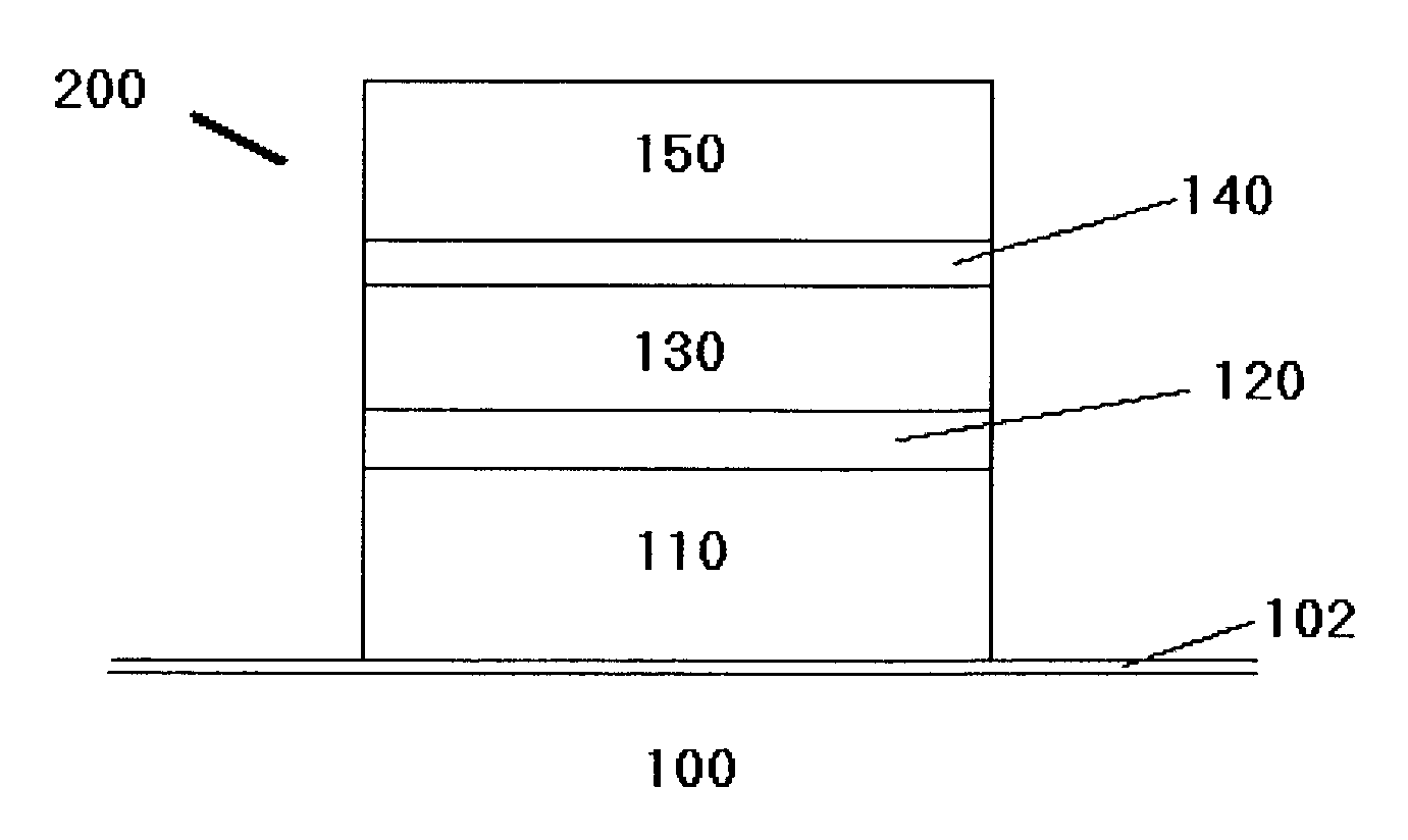
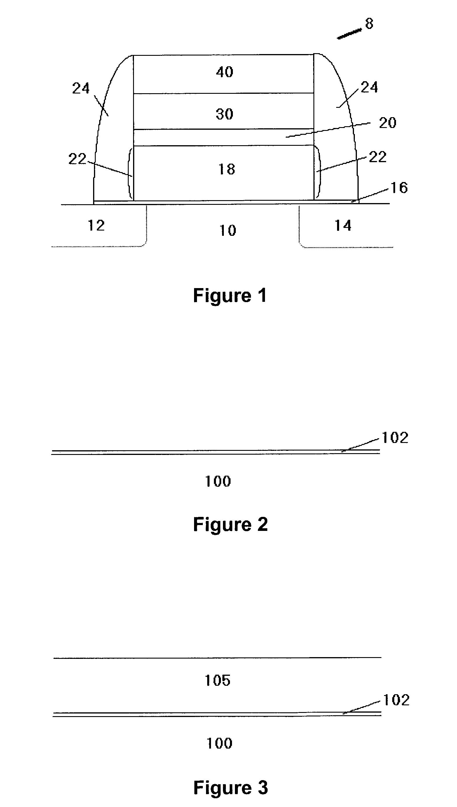
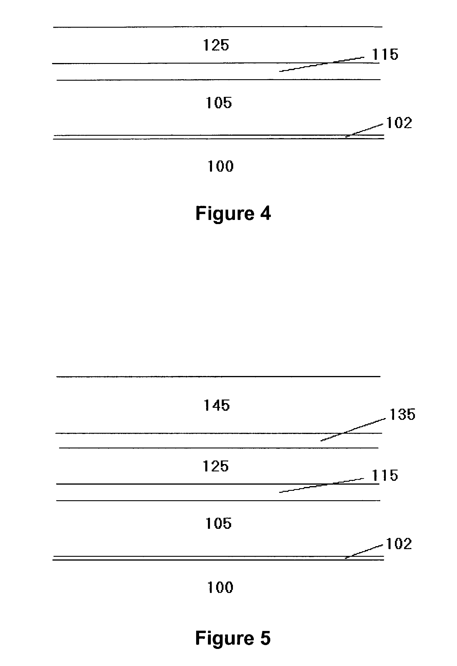
Image

Examples
example
Example 1
Formation of a Gate Structure
[0043]The following detailed steps were used to form the gate stack having a split gate:
[0044]
Nitrogen-containing gate oxide formationPoly deposition - single amorphous gate depositMask for P-dopingP+ poly implantationN-well implantationP-channel implantationP+ poly implantation strip resistMask for N-dopingP-well implantationN+ poly implantationN-channel implantationN+ poly implantation strip resistTungsten gate pre-cleanTungsten PVD, sputtering (nitrogen+argon, then argon only)Nitride - PECVDDeposit ARC and ResistEtch mask for nitrideNitride etch - ARC, silicon nitride, and partialtungsten etchRemove resistTungsten and Poly etchPost-poly etch cleanSelective oxidationN+ source / drain extension implantStripping & cleaningP+ source / drain extension implantStripping & cleaningNitride spacer deposition (BTBAS chemistry)Spacer etchPost-spacer etch cleanN+ source / drain implantStripping & cleaningP+ source / drain implantStripping & cleaningNitride-poly c...
PUM
 Abstract
Description
Claims
Application Information