Sequential gas flow oxide deposition technique

a gas flow oxide and evaporation technology, applied in the field of evaporation gas flow oxide deposition technique, can solve the problems of slow growth of materials, adverse effects on device operation, and inability of semiconductor manufacturers to completely fill,

Inactive Publication Date: 2008-07-15
APPLIED MATERIALS INC
View PDF31 Cites 469 Cited by
  • Summary
  • Abstract
  • Description
  • Claims
  • Application Information

AI Technical Summary

Problems solved by technology

Gaps having a combination of a high aspect ratio and a small width present a challenge for semiconductor manufacturers to fill completely.
In short, the challenge usually is to prevent the film from forming in a manner that closes off the gap before it is filled.
Failure to fill a gap completely results in the formation of a void in the deposited layer, which may adversely affect device operation.
Thus, the filling of trenches 24 is typically one of the most challenging gapfill applications in the formation of the integrated circuit.
As can be appreciated, such ALD techniques typically result in a very controlled, slow growth of material.
Despite the efforts of these researches, however, to the best of the inventor's knowledge, no one has developed an ALD silicon oxide process to deposit relatively thick oxide layers such as those required in shallow trench isolation and other gapfill applications, suitable for commercial use.

Method used


Image

  • Sequential gas flow oxide deposition technique
  • Sequential gas flow oxide deposition technique
  • Sequential gas flow oxide deposition technique

Examples


Embodiment Construction

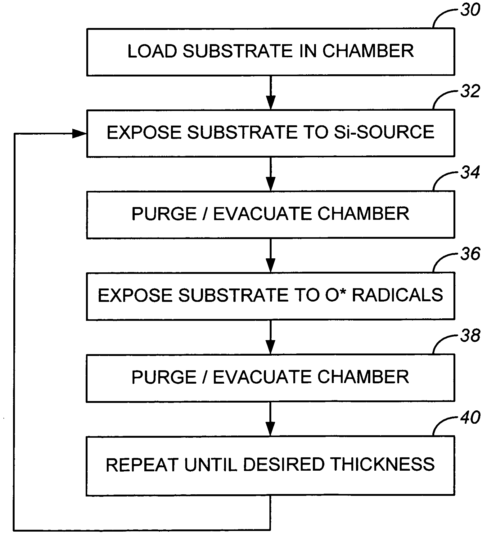
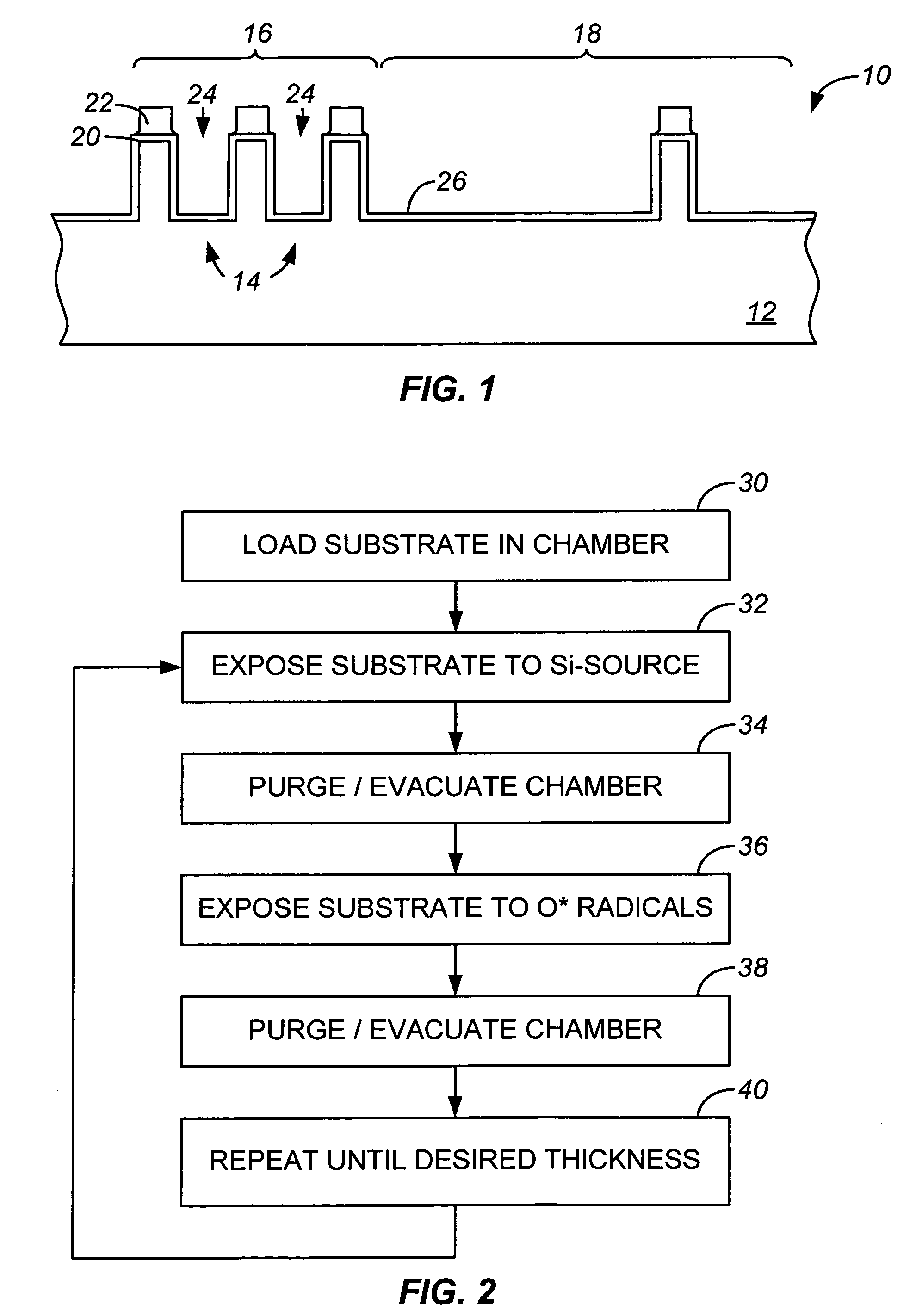
[0018]Embodiments of the invention pertain to a process for depositing a silica glass dielectric material using ALD techniques. Some embodiments of the invention permit the dielectric material to be deposited into closely-spaced gaps with substantially 100% gap fill for most currently envisioned small-width, high aspect ratio applications. For example, for gaps having a width of 0.10 microns substantially 100% gapfill can be achieved by embodiments of the invention for aspect ratios of 8:1 and even higher in both the active and open areas of an integrated circuit die. Other embodiments of the invention are particularly useful for depositing blanket silica glass films having a high density and exhibiting good stochiometry. Embodiments of the invention are useful for a variety of different applications and are particularly useful for the fabrication of integrated circuits having minimum feature sizes of 0.10 microns or less.

[0019]In order to better appreciate and understand the presen...


PUM

PropertyMeasurementUnit
temperatureaaaaaaaaaa
aspect ratioaaaaaaaaaa

Abstract

A method of depositing a silica glass insulating film over a substrate. In one embodiment the method comprises exposing the substrate to a silicon-containing reactant introduced into a chamber in which the substrate is disposed such that one or more layers of the silicon-containing reactant are adsorbed onto the substrate; purging or evacuating the chamber of the silicon-containing reactant; converting the silicon-containing reactant into a silica glass insulating compound by exposing the substrate to oxygen radicals formed from a second reactant while biasing the substrate to promote a sputtering effect, wherein an average atomic mass of all atomic constituents in the second reactant is less than or equal to an average atomic mass of oxygen; and repeating the exposing, purging / evacuating and exposing sequence a plurality of times until a desired film thickness is reached.

Description

BACKGROUND OF THE INVENTION[0001]One of the primary steps in the fabrication of modern semiconductor devices is the formation of an insulation film on a semiconductor substrate. Such insulation films are used for a variety of purposes including, among others, separating adjacent conductive layers (e.g., an intermetal dielectric (IMD) layer separates adjacent metal lines while a premetal dielectric (PMD) layer separates metal layer one from the conductive substrate) and separating adjacent active regions of the substrate (e.g., as part of a shallow trench isolation (STI) structure).[0002]For applications such as the deposition of IMD or PMD layers in an integrated circuit or the formation of STI structures, one important physical property of the insulation film is its ability to completely fill gaps between adjacent structures without leaving voids within the gap. This property is referred to as the film's gapfill capability. Gaps that may require filling include spaces between adjac...

Claims


Application Information

Patent Timeline
Patent Type & Authority Patents(United States)
IPC IPC(8): C23C14/34C23C16/00C23C16/40C23C16/44C23C16/455C23C16/507
CPCC23C16/402C23C16/507C23C16/45542
Inventor MOGHADAM, FARHAD K.COX, MICHAEL S.KRISHNARAJ, PADMANABHANPHAM, THANH N.
Owner APPLIED MATERIALS INC
Why Eureka
Try Eureka