
Polysilazane perhydride solution and method of manufacturing a semiconductor device using the same

a technology of polysilazane perhydride and semiconductor devices, which is applied in the direction of semiconductor/solid-state device manufacturing, basic electric elements, electric apparatus, etc., can solve the problems of ozone burying, voids or seams, and teos cvd-sio,

Active Publication Date: 2008-08-05
KIOXIA CORP
View PDF5 Cites 7 Cited by
  • Summary
  • Abstract
  • Description
  • Claims
  • Application Information

AI Technical Summary

Problems solved by technology

Recently however, due to the increase in aspect ratio of the trench for meeting demands for enhancing the fineness of semiconductor elements, it is now becoming increasingly difficult to bury the conventional ozone (O3)-TEOS CVD-SiO2 film or HDP CVD-SiO2 film in the trench of STI structure without causing the generation of voids or a seam.
On the occasion of the hydrolysis and dehydrocondensation reaction of silanol however, a large magnitude of volumetric shrinkage generated in the coated film, resulting in the generation of cracks in the silicon dioxide film filled in the STI trench.

Method used


Image

  • Polysilazane perhydride solution and method of manufacturing a semiconductor device using the same
  • Polysilazane perhydride solution and method of manufacturing a semiconductor device using the same
  • Polysilazane perhydride solution and method of manufacturing a semiconductor device using the same

Examples


embodiment 1

[0049]This embodiment illustrates one example of a burying method for STI, which will be explained with reference to FIGS. 7 to 10.

[0050]First of all, a silicon dioxide film (about 10 nm in thickness) 11 was formed on a silicon substrate 10 by thermal oxidation. Then, by a vacuum CVD method, a silicon nitride film (about 200 nm in thickness) 12 was formed, as a CMP stopper film, on the silicon dioxide film 11. The film thickness of the film to be formed on the substrate may be altered. For example, the film thickness of the CMP stopper film 12 may be varied within the range of about 100-300 nm.

[0051]By photolithography and a dry etching method, an element isolation trench (STI trench) 13 was formed so as to enable the STI trench 13 to pass through the CMP stopper film 12 and the silicon dioxide film 11 and to reach the silicon substrate 10 as shown in FIG. 7. Herein, the configuration of the STI trench 13 was 100 nm in width and 500 nm in depth. However, the width and depth of the S...

embodiment 2

[0059]In the same manner as described in the aforementioned Embodiment 1, a silicon dioxide film 16 was formed on an Si substrate 10 having a silicon dioxide film 11 and a CMP stopper film 12 formed thereon and also having an STI trench 13 formed thereon as shown in FIG. 9. These films were formed using the same materials as described in Embodiment 1, the film thickness of these films also being the same as described in Embodiment 1.

[0060]In this embodiment, the silicon dioxide film 16 was densified prior to the step of CMP. The densification of the silicon dioxide film 16 can be performed through the heat treatment thereof in an inert gas atmosphere at a temperature ranging from 700° C. to 1100° C. If the temperature of this heat treatment is lower than 700° C., it would become difficult to sufficiently densify the silicon dioxide film 16. On the other hand, if the temperature of this heat treatment is higher than 1100° C., the diffusion depth of the channel layer formed in advance...

embodiment 3

[0065]The densification of the silicon dioxide film 16 set forth in the above Embodiment 2 can be performed after the step of burying the silicon dioxide film 16 in the STI trench 13. In this embodiment, in the same manner as described in Embodiment 1, the silicon dioxide film 16 was buried in the STI trench 13 of the Si substrate 10 having a silicon dioxide film 11 and a CMP stopper film 12 formed thereon as shown in FIG. 10. Since the silicon dioxide film 16 was subjected to CMP prior to the densification thereof, the absolute quantity of polysilazane perhydride film was smaller than that of Embodiment 2 and hence the quantity of residual carbon was also smaller as compared with that of Embodiment 2. As a result, it would be advantageous in the respect that the properties of a device would hardly be deteriorated by the densification.

[0066]Then, the heat treatment was performed under the same conditions as in Embodiment 2 to densify the silicon dioxide film 16. As a result, it was ...


PUM

PropertyMeasurementUnit
temperatureaaaaaaaaaa
widthaaaaaaaaaa

Abstract

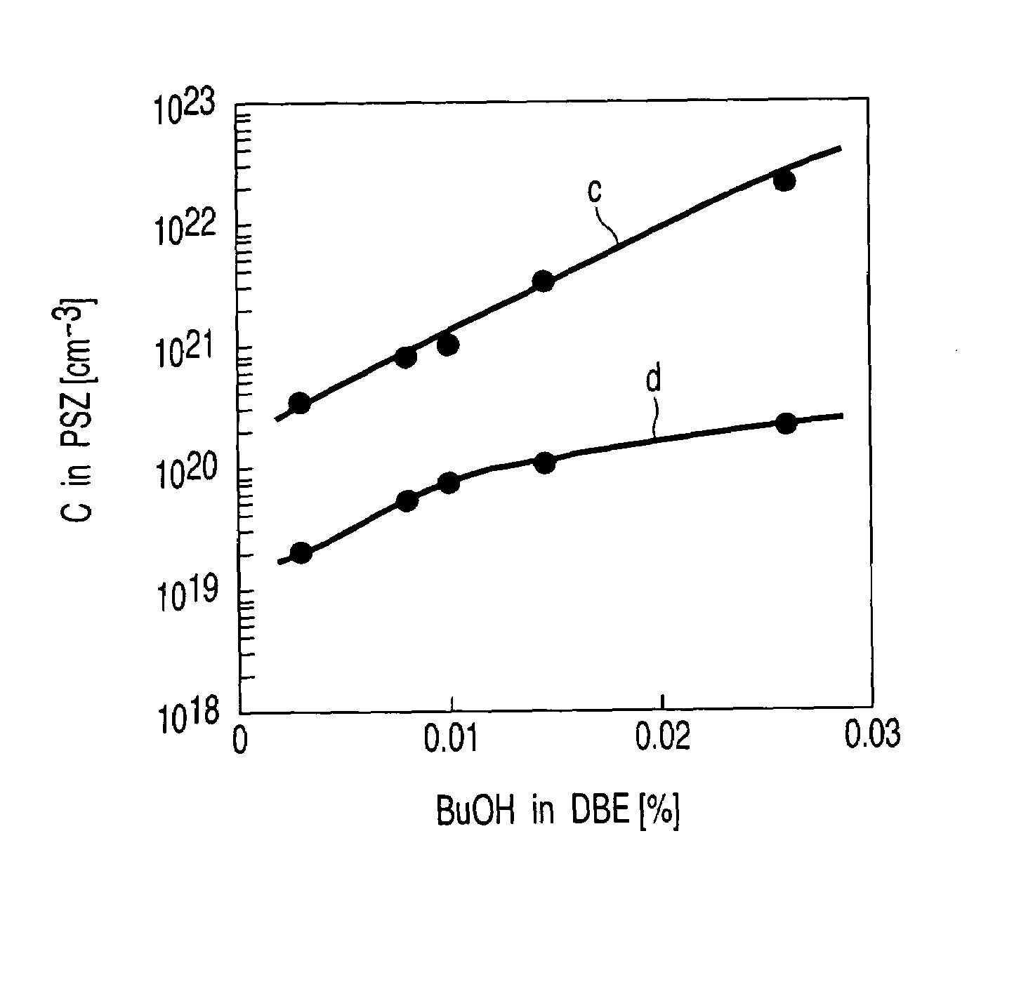
Disclosed is a method of manufacturing a semiconductor device comprising forming an element isolation trench in a semiconductor substrate, coating a polysilazane perhydride solution on the semiconductor substrate having the element isolation trench formed thereon to form a polysilazane perhydride film, the polysilazane perhydride solution comprising dibutyl ether having a butanol concentration of 30 ppm or less, and polysilazane perhydride dissolved in the dibutyl ether, subjecting the polysilazane perhydride film to oxidation in an atmosphere containing water vapor to form a silicon dioxide film, and selectively removing the silicon dioxide film to leave the silicon dioxide film in the element isolation trench to form an element isolating insulation film.

Description

CROSS-REFERENCE TO RELATED APPLICATIONS[0001]This application is based upon and claims the benefit of priority from prior Japanese Patent Application No. 2005-065811, filed Mar. 9, 2005, the entire contents of which are incorporated herein by reference.BACKGROUND OF THE INVENTION[0002]1. Field of the Invention[0003]This invention relates to a polysilazane perhydride solution and a method for manufacturing a semiconductor device by using a polysilazane perhydride solution.[0004]2. Description of the Related Art[0005]An isolation structure known as an STI (Shallow Trench Isolation) structure is extensively employed for the isolation of elements in a semiconductor device. This STI structure can be created by a method wherein a trench is formed in an element isolation region of a semiconductor substrate, and then, a silicon oxide (SiO2) film functioning as an element isolating insulation film is buried inside this trench to form this STI structure. Recently however, due to the increase ...

Claims


Application Information

Patent Timeline
Patent Type & Authority Patents(United States)
IPC IPC(8): H01L21/76
CPCH01L21/02164H01L21/02222H01L21/02282H01L21/76224H01L21/31053H01L21/3125H01L21/316H01L21/02337
Inventor KAWASAKI, ATSUKOKIYOTOSHI, MASAHIRONAKAZAWA, KEISUKEARISUMI, OSAMUHOSHI, TAKESHITACHIBANA, KATSUHIKO
Owner KIOXIA CORP
Learn More