Control of output beam divergence in a semiconductor waveguide device

a semiconductor waveguide and output beam technology, applied in semiconductor lasers, instruments, optical elements, etc., can solve the problems of difficult to achieve high kink-free emission power, low coupling tolerance between laser and single-mode fibre, and high coupling loss to optical components, so as to reduce beam divergence

Active Publication Date: 2008-08-05
INTENSE LTD
View PDF16 Cites 2 Cited by
  • Summary
  • Abstract
  • Description
  • Claims
  • Application Information

AI Technical Summary

Benefits of technology

[0015]It is an object of the present invention to provide a semiconductor waveguide device with reduced beam divergence in the vertical direction.

Problems solved by technology

The very large far field and asymmetry of the far fields in the vertical and horizontal directions cause a number of problems such as high coupling loss to optical components downstream of the laser output 17 (such as optical fibres) and particularly low coupling tolerance between the laser and a single mode fibre (which requires a circular beam profile).
In addition, it becomes more difficult to achieve high kink-free emission power due to the occurrence of higher mode lasing at high current injection levels.

Method used


Image

  • Control of output beam divergence in a semiconductor waveguide device
  • Control of output beam divergence in a semiconductor waveguide device
  • Control of output beam divergence in a semiconductor waveguide device

Examples


Embodiment Construction

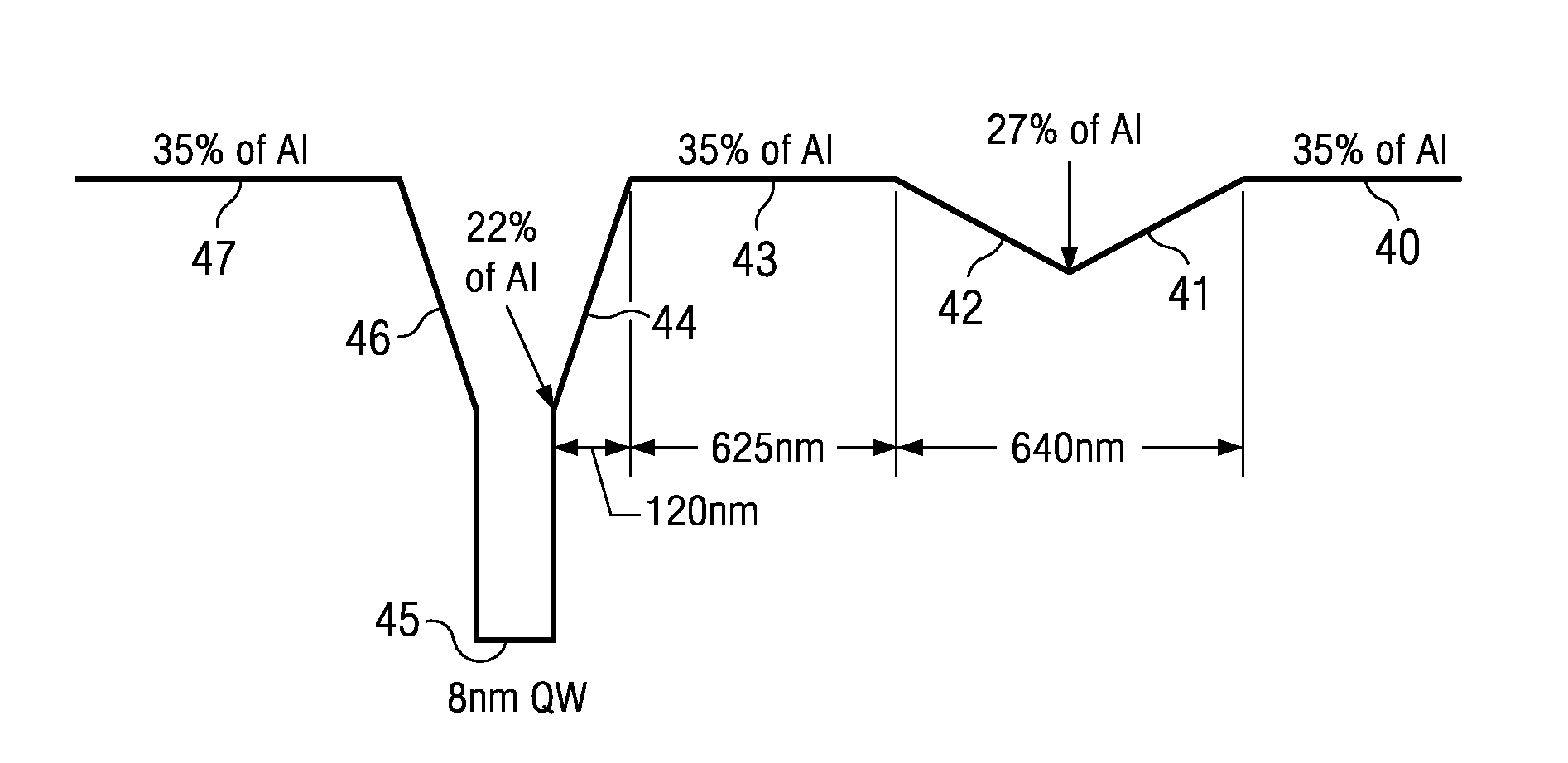
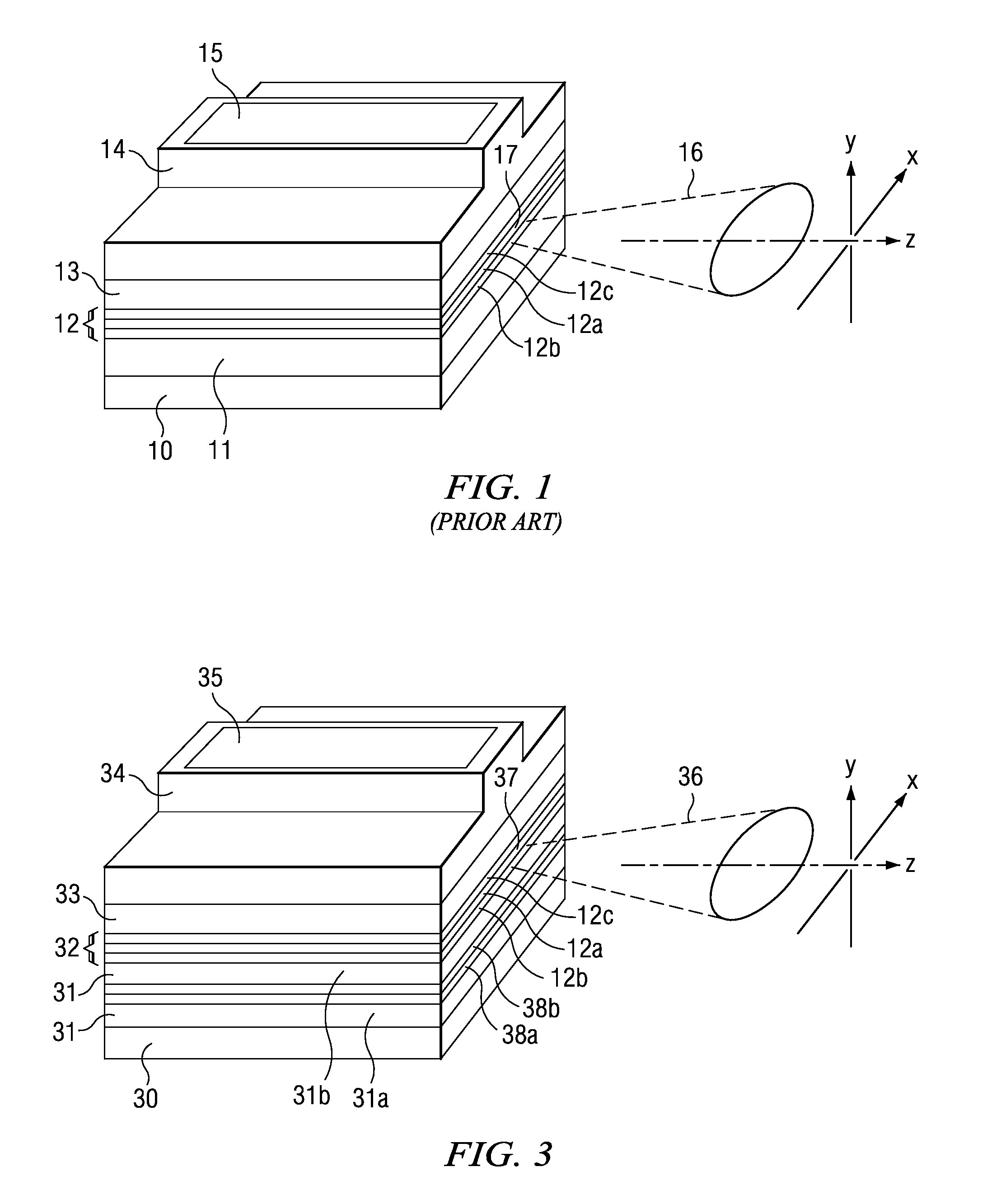
[0045]With reference to FIG. 3 a preferred configuration of device according to the present invention is shown schematically. A substrate 30 supports a lower cladding layer 31, an optically active core region 32 and an upper cladding layer 33. In the preferred arrangement, a ridge waveguide 34 provides lateral optical confinement. A suitable electrical contact material 35 may be deposited onto the ridge 34 with which to provide electrical injection to drive the lasing mode.

[0046]It is noted that the principles of the present invention may be applied to laser diodes having other forms of structure providing lateral optical confinement, such as a buried heterostructure laser. It is also noted that the principles of the present invention may also be applied generally to a semiconductor waveguiding structure other than a laser diode. More generally, the principles can be applied in active and passive optical devices with laterally confining waveguide structures. These include amplifiers...


PUM


Abstract

A semiconductor laser device incorporates a beam control layer for reducing far field and beam divergence. Within the beam control layer, a physical property of the semiconductor material varies as a function of depth through, the beam control layer, by provision of a first sub-layer in which the property varies gradually from a first level to a second level, and a second sub-layer in which the property varies from said second level to a third level. In the preferred arrangement, the conduction band edge of the semiconductor has a V-shaped profile through the beam control layer.

Description

BACKGROUND OF THE INVENTION[0001]The present invention relates to semiconductor waveguide devices, and in particular to methods for controlling the optical output beam divergence therefrom.[0002]The invention has particular, though not exclusive, use in the manufacture of semiconductor lasers, amplifiers, modulators and other waveguides suitable for use in telecommunications and printing applications where low coupling loss to other optical components (such as optical waveguides) and high kink-free power output is required. More particularly, the invention has particular, though not exclusive, use in the manufacture of 980 nm pump lasers for telecommunications applications, and in the manufacture of 830 nm high power lasers for printing applications.[0003]Conventional semiconductor lasers generally provide an optical output beam of substantially elliptical cross-section. With reference to FIG. 1, such conventional lasers typically comprise a succession of layers formed on a substrat...

Claims


Application Information

Patent Timeline
Patent Type & Authority Patents(United States)
IPC IPC(8): G02B6/10H01S3/10H01S5/00G02B6/122H01S5/223H01S5/32H01S5/34H01S5/343
CPCB82Y20/00G02B6/122G02B6/1228H01S5/2231H01S5/0655H01S2301/18H01S5/3215H01S5/3407H01S5/34366
Inventor QIU, BOCANG
Owner INTENSE LTD
Why Eureka
Try Eureka