Thin-film transistor and fabrication method thereof

a thin-film transistor and fabrication method technology, applied in the direction of basic electric elements, electrical equipment, semiconductor devices, etc., can solve the problems of affecting the electric property the formation cost of the normal photomask is twice as high, and the formation cost of the formation cost of the normal photomask is double the formation cost of the normal photomask, etc., to avoid the occurrence of photo current, improve the quality of the thin-film transistor, and reduce the number of photomasks

Active Publication Date: 2008-08-19
AU OPTRONICS CORP
View PDF16 Cites 19 Cited by
  • Summary
  • Abstract
  • Description
  • Claims
  • Application Information

AI Technical Summary

Benefits of technology

[0010]It is therefore a primary objective of the present invention to provide a thin-film transistor structure and a fabrication method thereof through a laser ablation process for solving the above-mentioned problems of high cost and photo current of the prior-art method for fabricating thin-film transistors.
[0013]It is an advantage of the claimed invention that the fabrication method of thin-film transistors simultaneously etching the first conductive layer, the first insulating layer, the semiconductor layer, and the second conductive layer, so that there is no semiconductor layer existing below most portions of data lines, which effectively avoids the occurrence of photo current and improves the quality of the thin-film transistor. Furthermore, the claimed invention method utilizes a laser ablation process to define the channel pattern of the semiconductor island such that at least a photolithography process can be omitted. As a result, the number of photomasks utilized during the fabrication method may be reduced, and the process cost can be effectively lowered while forming thin-film transistors with good qualities.

Problems solved by technology

Because the size of the channel pattern of the thin-film transistor is very detailed and minute, the half-tone mask for defining the channel pattern by its half-tone region has to be very accurate, whose formation cost is very high and is twice as the formation cost of normal photomask.
In addition, once a defect of the transference of the channel pattern occurs during the second PEP by using a half-tone mask, it will seriously affect the electric property of the thin-film transistor, which is hard to be repaired.
Furthermore, according to the prior-art process of fabricating a thin-film transistor, both of the source and drain patterns cover the semiconductor layer so that photo current is easily induced since most materials of the semiconductor layer are amorphous silicon materials that have photo sensitivity, and photo current affects the electrical performance of the thin-film transistor.
Therefore, how to fabricate thin-film transistors with good qualities by low-cost processes to avoid the photo current problem is still an important issue for the manufactures.

Method used


Image

  • Thin-film transistor and fabrication method thereof
  • Thin-film transistor and fabrication method thereof
  • Thin-film transistor and fabrication method thereof

Examples


first embodiment

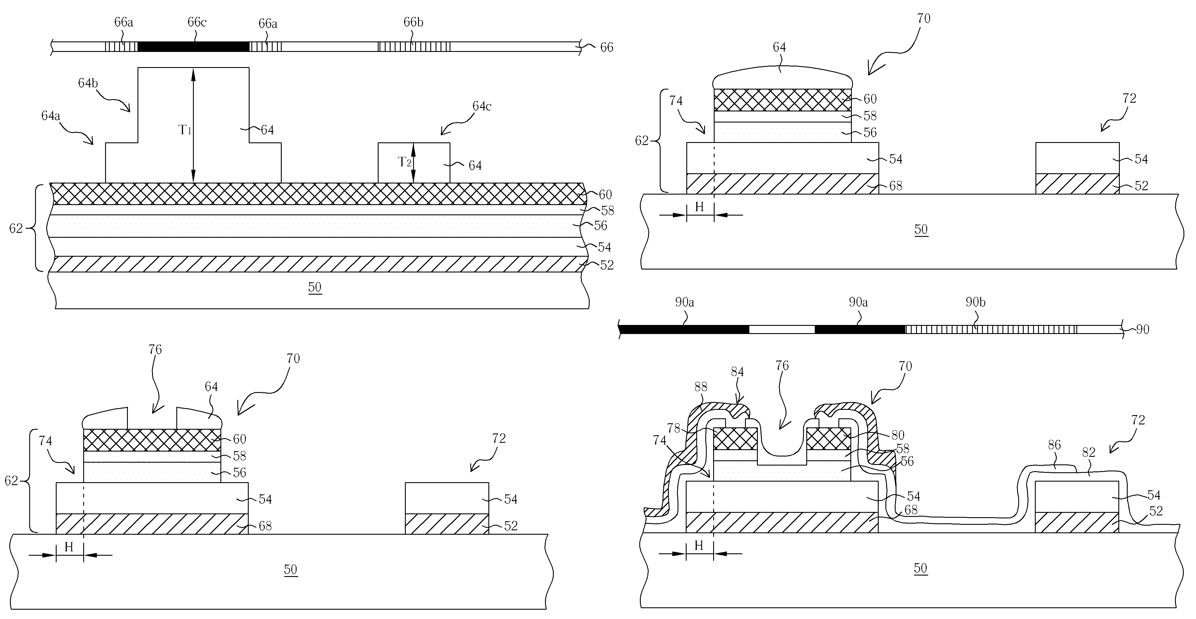
[0018]FIGS. 5-11 are schematic diagrams of the fabrication process of a thin-film transistor according to the present invention. Referring to FIG. 5, first, a transparent substrate 50 is provided, wherein the substrate 50 may be a glass substrate, a quartz substrate, or a plastic substrate. Then, four thin films 62 are successively formed on the surface of the substrate 50, and the four thin films 62 comprises a first conductive layer 52, an insulating layer 54, a semiconductor layer 56, and a second conductive layer 60 from bottom to top. However, during forming the four thin films 62, an ohmic contact layer 58, such as an N+ doped layer, may be formed between the second conductive layer 60 and the semiconductor layer 56 in order to reduce the resistance between these two layers. In other words, the first conductive layer 52, the insulating layer 54, the semiconductor layer 56, the ohmic contact layer 58, and the second conductive layer 60 are successively formed on the surface of ...

second embodiment

[0023]Referring to FIGS. 12-13, FIGS. 12-13 are schematic diagrams of the fabrication process of a thin-film transistor according to the present invention. FIG. 12 is a continuation of the fabrication process of FIG. 6. After the first PEP, a semiconductor island 70, a gate electrode 68, and a wire structure 72 are formed on the surface of the substrate 50, wherein the areas of the gate electrode 68 and the insulating layer 54 are both larger than the area of the semiconductor island 70 so that stair structures 74 are formed at two sides of the four thin films 62 to contribute to form the passivation layer on the semiconductor island 70, which may uniformly step cover the surfaces of the whole semiconductor island 70 and the gate electrode 68. The photoresist layer 64 is removed after the first PEP.

[0024]Thereafter, as shown in FIG. 13, a laser ablation process is carried out to the semiconductor island 70 to directly remove a portion of the second conductive layer 60 so as to defin...


PUM

PropertyMeasurementUnit
widthaaaaaaaaaa
conductiveaaaaaaaaaa
areasaaaaaaaaaa

Abstract

A fabrication method of a TFT includes successively forming four thin films containing a first conductive layer, an insulation layer, a semiconductor layer, and a second conductive layer on a substrate, performing a first PEP process to pattern the four thin films for forming a semiconductor island and a gate electrode with the semiconductor layer and the first conductive layer respectively. Then, a laser ablation process is performed to define a channel pattern in the four thin films and remove a portion of the second conductive layer so that unconnected source electrode and drain electrode are formed with the second conductive layer.

Description

BACKGROUND OF THE INVENTION[0001]1. Field of the Invention[0002]The present invention relates to a thin-film transistor (TFT) structure and a fabrication method thereof, and more particularly, to a TFT structure and a fabrication method with a laser ablation process.[0003]2. Description of the Prior Art[0004]Due to the continued development in technology, flat displays have been widely used in various information products. Common flat displays comprise liquid crystal displays (LCD), organic light-emitting displays (OLED), and plasma display panels (PDP). Among the various types of flat displays, LCDs are developed maturely. Because TFT-LCDs have qualities of light weight, thinness, low energy requirements, and no radiation, they have been widely used in portable information products, such as notebook computers, personal digital assist (PDA), and mobile phones. Conventionally, the main electric elements of a LCD are thin-film transistors arranged as an array. In operation with approp...

Claims


Application Information

Patent Timeline
Patent Type & Authority Patents(United States)
IPC IPC(8): H01L21/84H01L21/336
CPCH01L29/66765H01L27/1214H01L27/1288
Inventor LIN, HAN-TU
Owner AU OPTRONICS CORP
Why Eureka
Try Eureka