System in-package test inspection apparatus and test inspection method

a technology of in-package test and inspection apparatus, which is applied in the direction of individual semiconductor device testing, basic electric elements, instruments, etc., can solve the problems of inability to accurately inspect and delay the preparation process, and achieve the effect of excellent transmission of high frequency signals and reduced inductance within the lsi packag

Inactive Publication Date: 2008-08-19
NAT INST OF ADVANCED IND SCI & TECH
View PDF17 Cites 2 Cited by
  • Summary
  • Abstract
  • Description
  • Claims
  • Application Information

AI Technical Summary

Benefits of technology

[0012]The present invention has been achieved in views of the above-described situations and an object of the invention is to provide a system in-package test inspection apparatus in which upon manufacturing of the chip stack type SIP, high-speed, high-frequency test inspection is carried out by inputting an inspection signal from signal lines between the LSI chips so as to execute acceptable product inspection at a high precision, thereby securing reliability.
[0015]By using the probe capable of contacting the signal line between the LSI chips stacked in multiple layers on the system in-package and further, using the printed wiring board capable of handling the high-speed / high-frequency signal, the high-speed / high-frequency test inspection can be carried out at a high precision. That is, the inspection signal can be inputted to the LSI chip not through the metallic wiring formed within the LSI package, so that influences of inductance within the LSI package can be reduced largely thereby high frequency signal being transmitted excellently.
[0016]Therefore, on the manufacturing site of the system in-package, implementation of acceptable product inspection and securing of reliability can be achieved.
[0018]Consequently, signals in the high-speed, high frequency area can be transmitted and further, influences of cross-talk between respective signal lines and external noise can be reduced.
[0021]According to these methods, the same effect as the aforementioned system in-package test inspection apparatus can be obtained. That is, because the inspection signal is inputted to the LSI chip not through the metallic wiring formed within the LSI package, influences of inductance within the LSI package can be reduced largely and the high frequency signal can be transmitted excellently. Therefore, the high speed / high frequency test inspection can be carried out at a high precision so that implementation of acceptable product inspection and securing of reliability can be achieved on the manufacturing site of the system in-package.

Problems solved by technology

Although the test inspection on the aforementioned package stack type and plane multi-chip type can be met by conventional technology, the chip stack type SIP which can be expected to reduce cost largely in the SIPs and is estimated to prevail rapidly has not been yet developed from viewpoints of high speed / high frequency test inspection technology.
However, in the inspection of the high-speed / high-frequency characteristic, no high frequency signal can be transmitted due to an influence of inductance originating form a long wire within the LSI package 201, so that no accurate inspection is enabled.

Method used


Image

  • System in-package test inspection apparatus and test inspection method
  • System in-package test inspection apparatus and test inspection method
  • System in-package test inspection apparatus and test inspection method

Examples


Embodiment Construction

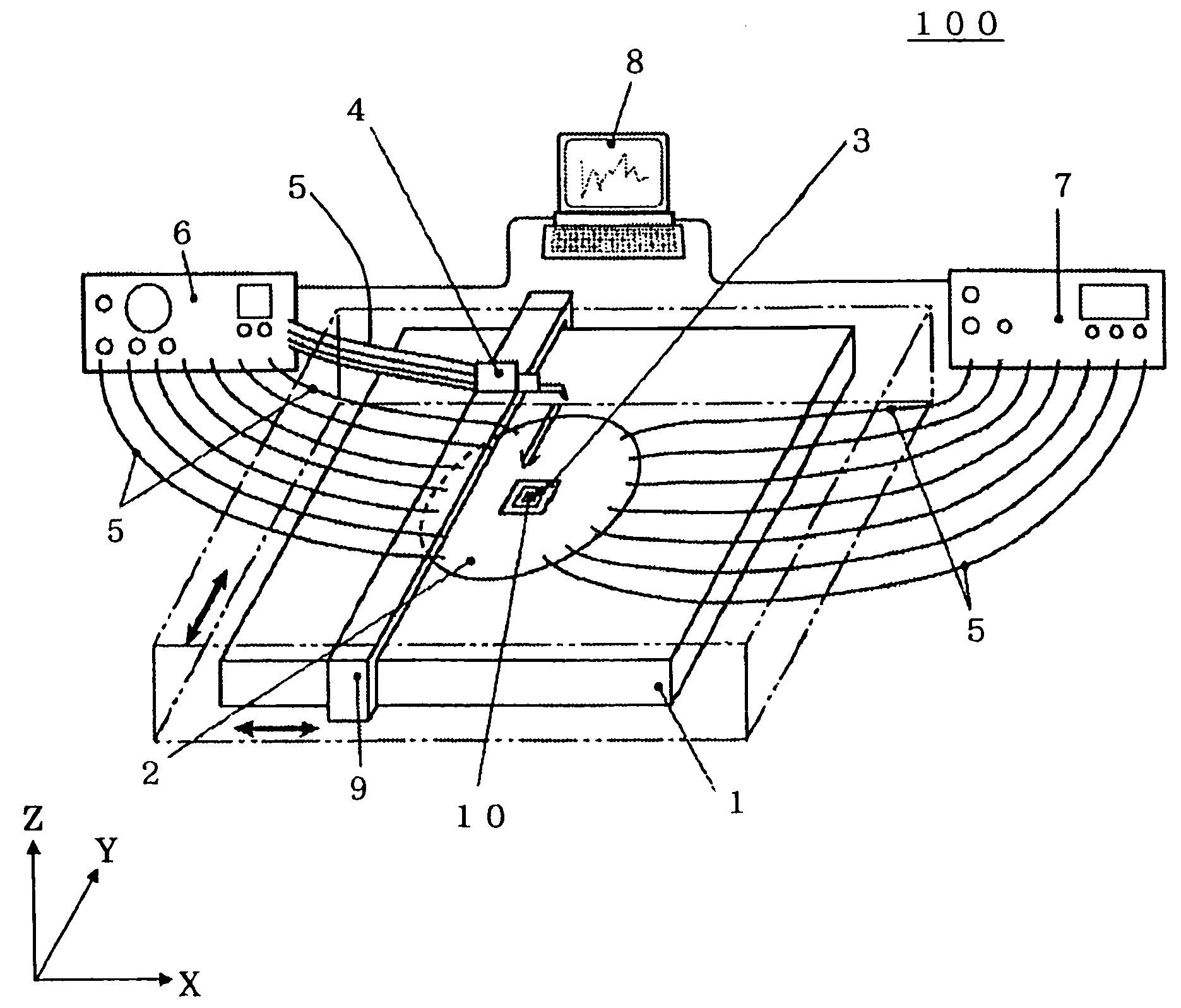
[0030]Hereinafter, the preferred embodiments of the present invention will be described with reference to the accompanying drawings. FIG. 1 is a perspective view showing the entire structure of the system in-package test inspection apparatus (hereinafter referred to as SIP test inspection apparatus) of the present invention.

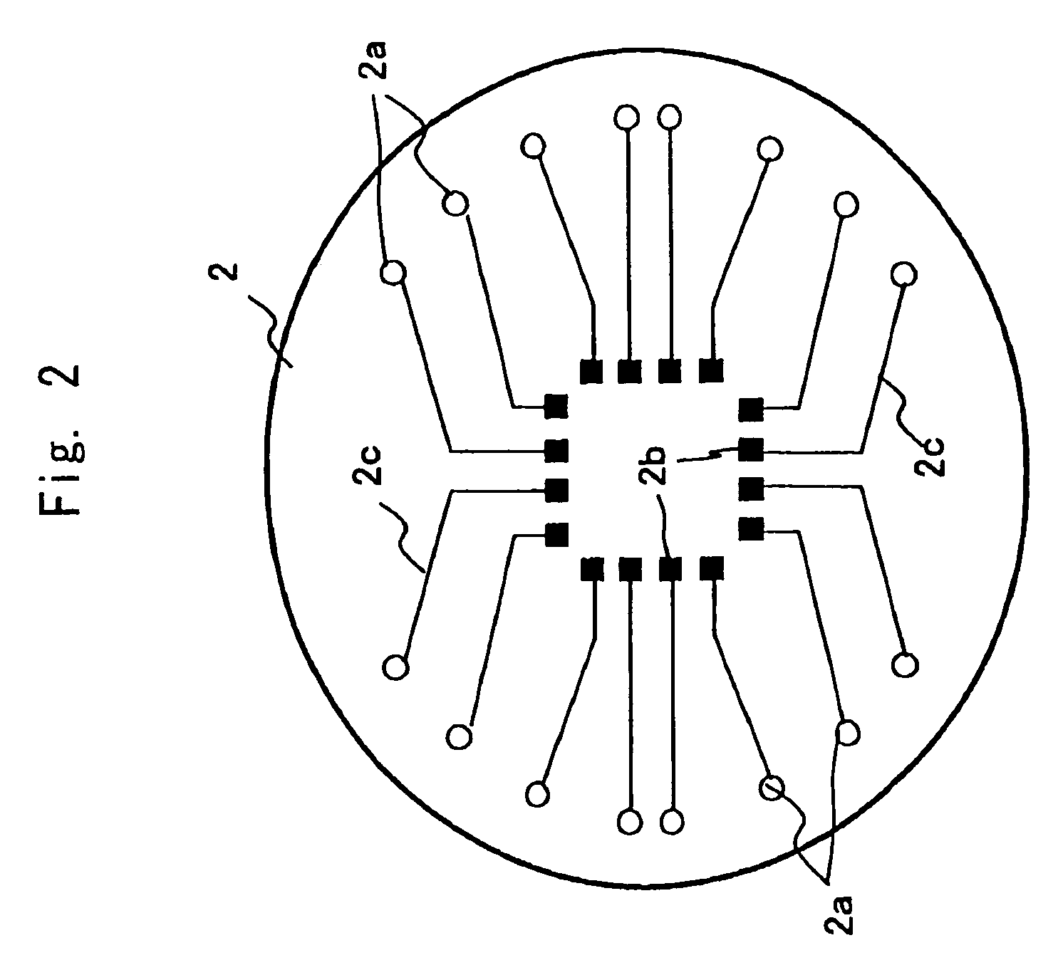
[0031]The SIP test inspection apparatus 100 shown in the same Figure has a high precision movable stage 1 which is movable at high precision in three directions, X, Y and Z-axes and a test card 2 is mounted on this high precision movable stage 1 as a printed wiring board capable of transmitting high velocity / high frequency signals. Further, a SIP socket 3 on which a system in-package (called SIP) of measuring object is mounted is loaded on the test card 2.

[0032]This SIP test inspection apparatus 100 includes an SIP evaluation signal generating device 6 (evaluation signal generating means) for generating an evaluation signal for inspection and a fine high frequenc...


PUM


Abstract

A system in-package test inspection apparatus for measuring and evaluating the high-speed / high frequency characteristic of a system in-package through an electrode pad in which I / O terminals are formed on one side of an LSI package containing metallic wiring internally and plural LSI chips are stacked in multiple layers on the other face while electric connection between the LSI chip and the LSI package and the electric connection between the LSI chips are implemented, the system in-package test inspection apparatus comprising: a printed wiring substrate to which the I / O terminals of the system in-package are connected to enable transmission of high speed and high frequency signals; LSI chip driving means for driving the LSI chip; a contact probe having a contact electrode and for transmitting a high frequency signal; evaluation signal generating means for supplying a high frequency evaluation signal to the contact probe; output signal detecting means for detecting an output signal of the system in-package through the printed wiring board; and analyzing means for analyzing a signal detected by the output signal detecting means, wherein by contacting the contact electrode of the contact probe with an electrode pad formed on the LSI chip, the evaluation signal is inputted to the LSI chip not through metallic wiring within the LSI package.

Description

BACKGROUND OF THE INVENTION[0001]1. Field of the Invention[0002]The present invention relates to a mounting technology of electronic information transmission system and more particularly to a system in-package test inspection apparatus for measuring and evaluating high-speed / high frequency electric characteristic of a system in-package (SIP) whose system is established on a structure body loaded with a multiplicity of electronic components such as semiconductor integrated circuit (LSI) chips and the like and a test inspection method.[0003]2. Description of the Related Art[0004]The system in-package (hereinafter referred to as SIP) concerns technology for mounting a plurality of LSI chips in a single package and because high density and high speed electronic system can be constructed using an existing LSI chip, application development thereof onto ubiquitous high function information devices such as mobile phone has been advanced energetically. If classified depending on the configur...

Claims


Application Information

Patent Timeline
Patent Type & Authority Patents(United States)
IPC IPC(8): G01R31/26G01R1/073G01R31/28H01L23/48
CPCG01R31/2822H01L2224/16225H01L2224/48091H01L2224/48137H01L2224/48145H01L2924/15311H01L2224/48227H01L2924/15192H01L2924/00014H01L2224/05573H01L2224/05568H01L2224/05599H01L2924/00012
Inventor AOYAGI, MASAHIRONAKAGAWA, HIROSHITOKORO, KAZUHIKOKIKUCHI, KATSUYAOKADA, YOSHIKUNIFUJITA, HIROYUKIKOBAYASHI, KENICHI
Owner NAT INST OF ADVANCED IND SCI & TECH
Why Eureka
Try Eureka