

Methods of processing nanocrystals, and compositions, devices and systems including same
a technology of nanocrystals and compositions, applied in the field of nanostructures, to achieve the effect of improving efficiency
- Summary
- Abstract
- Description
- Claims
- Application Information
AI Technical Summary
Benefits of technology
Problems solved by technology
Method used
Image

Examples
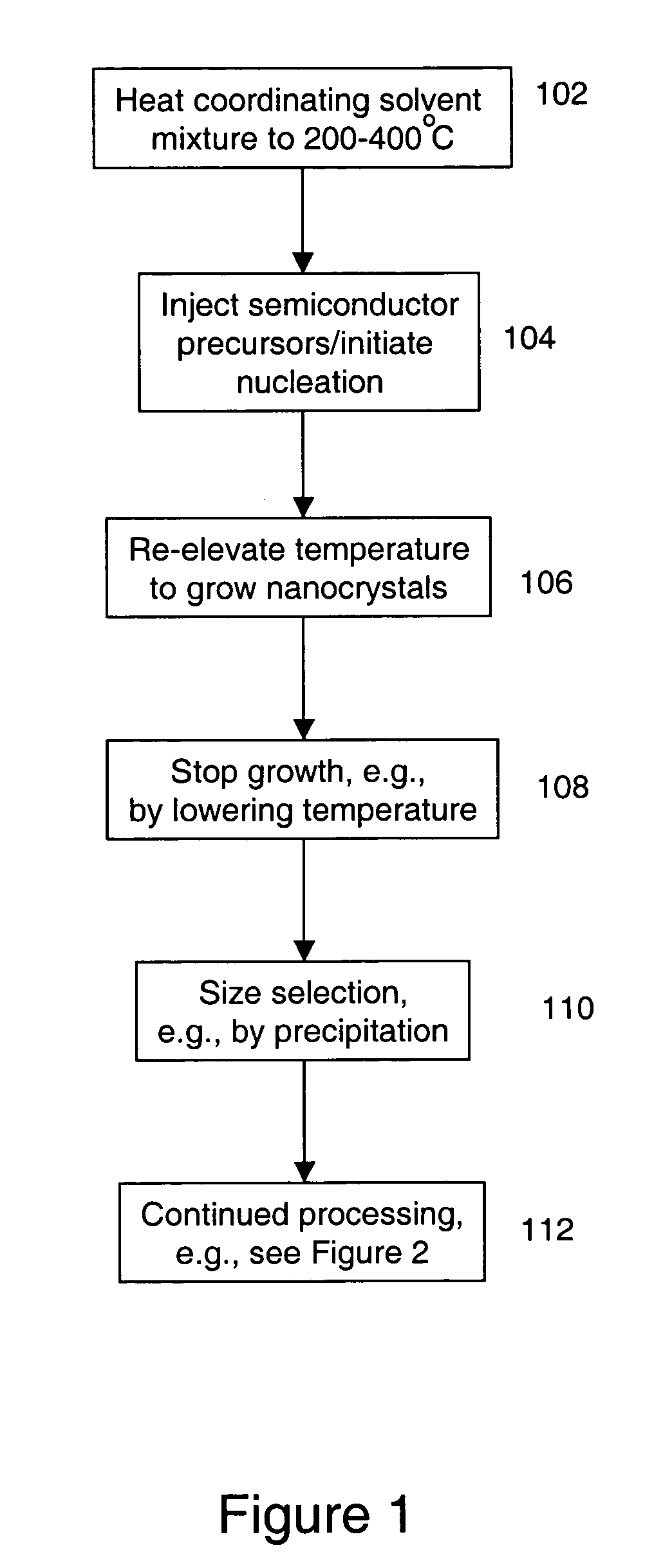
example 1
[0113]High purity nanocrystals were synthesized according to the following procedure. Due to high variability from manufacturer to manufacturer, surfactants for use in the synthesis process, e.g., HPA, TOPO and TDPA, were first checked for purity using standard NMR. If found to be less than 90% pure, the surfactants were purified by washing with CHCl3, dissolution and recrystallization using CHCl3 and hexanes until the desired purity was achieved. Once sufficiently pure reagents were available, the surfactants TOPO (3.54 g), TDPA (0.33 g) and HPA (0.13 g) were heated to 120° C., at which time the cadmium precursor (Cd(Me)2, 0.5 g of stock solution including 32% Cd(Me)2 by weight in TBP) was added to the mixture. The mixture was then heated to 360° C. and 2.5 g of the second precursor stock solution (e.g., Se:TBP (7.78% by weight)) was added, which dropped the reaction temperature to between 290° and 300° C. Crystals were then allowed to grow at this temperature for 5 minutes. The re...
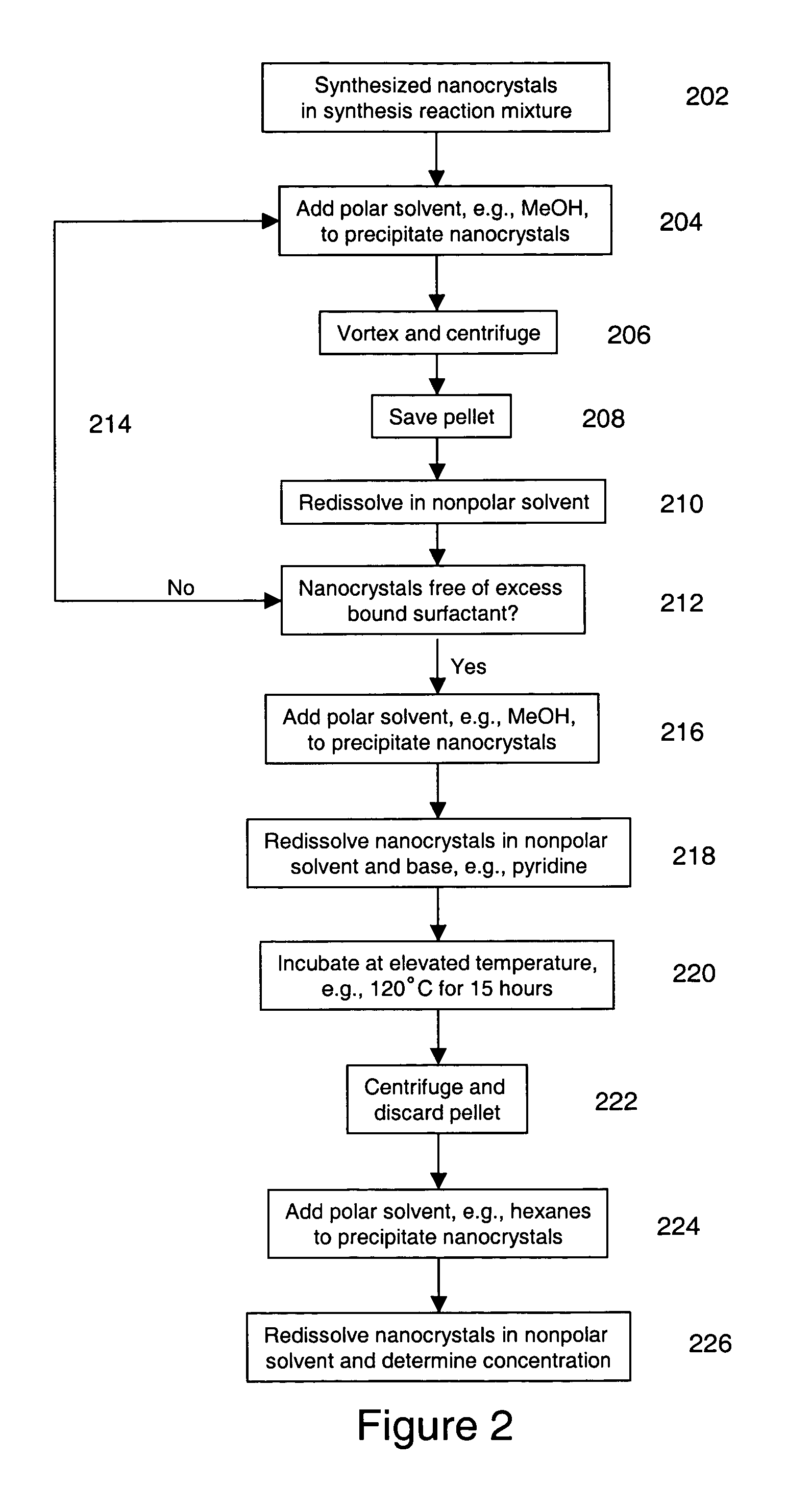
example 2
[0115]Excess organic surfactants such as trioctyl phosphine (TOP), trioctyl phosphine oxide (TOPO), hexadecyl phosphonic acid (HDPA), octadecyl phosphonic acid (ODPA), and tri-n-butyl phosphine (TBP) are commonly present in nanostructure preparations as prepared by standard techniques cited herein or in U.S. patent application Ser. No. 10 / 656,802. Optionally, any excess organic surfactant is removed from the nanostructure preparation prior to use of the nanostructures, for example, prior to their association with the conductive compositions described in U.S. patent application Ser. No. 10 / 656,802. This can be achieved, for example, by adding a solvent mixture prepared from a first solvent in which a nanostructure is soluble (e.g., toluene or chloroform) and a second solvent in which the nanostructure is not soluble (e.g., isopropanol or longer chain alcohol, or an acetate such as ethyl acetate). While the ratio of first solvent to second solvent as prepared in the solvent mixture ty...
example 3
[0118]This example describes fabrication of a photovoltaic device comprising two intermixed populations of processed nanocrystals, CdSe nanocrystals and CdTe nanocrystals. See U.S. patent application Ser. No. 10 / 656,910.
[0119]Substrate Cleaning
[0120]Substrates (e.g., ITO on glass, from Thin Film Devices, Inc., www.tfdinc.com) are cleaned, e.g., using the following procedure. Substrates are wiped with isopropanol, ultrasonicated in isopropanol, ultrasonicated in 2% Hellmanex™ deionized water, rinsed very thoroughly under flowing deionized water, ultrasonicated in deionized water, ultrasonicated in semiconductor grade acetone, and ultrasonicated in semiconductor grade isopropanol. Each sonication is for 15 minutes. The substrates are then oxygen plasma cleaned, at 200 W (1% reflected power) for 10 minutes with oxygen introduced at a pressure of approximately 400 mTorr into a vacuum of 80 mTorr.
[0121]PEDOT Layer Processing
[0122]PEDOT / PSS Poly(3,4-ethylenedioxythiophene) poly(styrenesul...
PUM
| Property | Measurement | Unit |
|---|---|---|
| angle | aaaaa | aaaaa |
| aspect ratio | aaaaa | aaaaa |
| aspect ratio | aaaaa | aaaaa |
Abstract
Description
Claims
Application Information