Power semiconductor device with a base region and method of manufacturing same

a technology of power semiconductor and base region, which is applied in the direction of semiconductor devices, basic electric elements, electrical appliances, etc., can solve the problems of unsatisfactory reliability of tested good devices, difficult to manufacture uniform cell structures across the entire mosfet, and improve the breakdown voltage. , to achieve the effect of improving channel density and on-state resistan

Active Publication Date: 2008-10-07
NXP USA INC
View PDF6 Cites 8 Cited by
  • Summary
  • Abstract
  • Description
  • Claims
  • Application Information

AI Technical Summary

Benefits of technology

[0021]Preferably, the power IGFET device is formed with individual cells having a plurality of sources regions separating said physically isolated drain regions such that these individual cells are packed into a relatively small area to contain at least 10 physically isolated drain cells to improve the channel density of the device.

Problems solved by technology

A second problem that is pertaining to the problem of increasing the channel density is the improvement of the breakdown voltage.
Because of the required minimum optical base cell shrinking process for lowering RDSON, it is not so straightforward to manufacture uniform cell structures across the entire MOSFET.
However, even if the breakdown voltage yield is impacted which consequently increases the final manufacturing cost, the reliability of the tested good devices is not fully guaranteed.
There is a risk of transistor failure for higher current density caused by the base cells during UIS testing.
However even if the P+ Body region is doped and located close to the beginning of the channel in such a way that the body resistor is dramatically reduced and provides a good immunity against a drop in tension which could activate the parasitic bipolar transistor, and lead to the device failure, it is still necessary to make sure that all individual cells structure are uniform within the entire MOSFET device.
It is far from straightforward to reduce the number of masking steps which can be used for every type of configuration.

Method used


Image

  • Power semiconductor device with a base region and method of manufacturing same
  • Power semiconductor device with a base region and method of manufacturing same
  • Power semiconductor device with a base region and method of manufacturing same

Examples


Embodiment Construction

[0035]The power semiconductor device in accordance with the present invention and a method for manufacturing thereof will now be described with reference to several illustrative applications and embodiments.

[0036]Although in the following description the layers and regions will be described as having certain conductivity types and being compared of certain materials, this is for illustrative purposes only. It is not intended that the invention be limited to the specific conductivity types or the specific materials referred to herein.

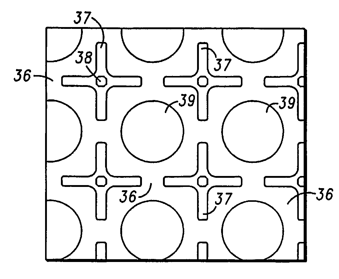
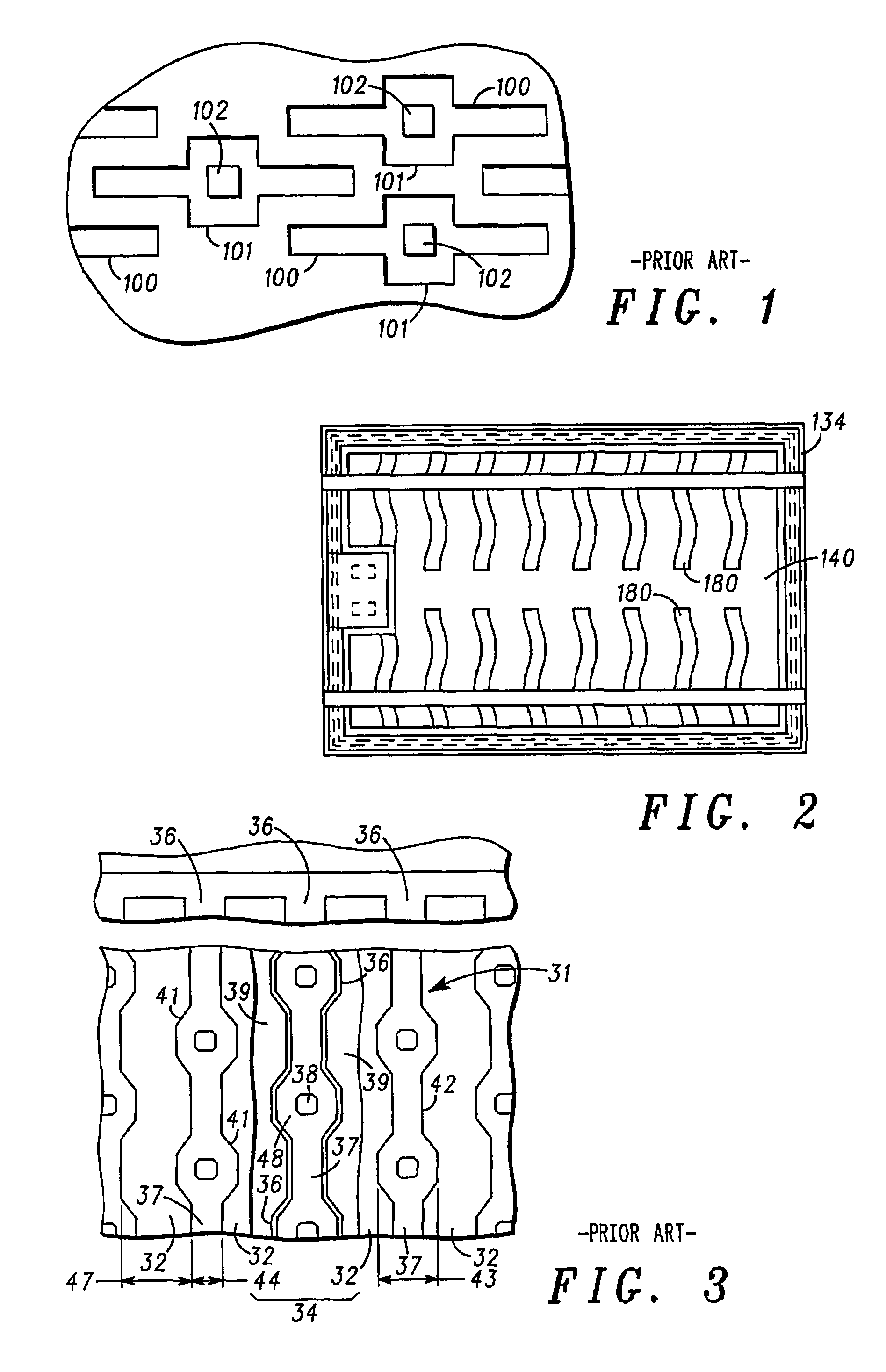
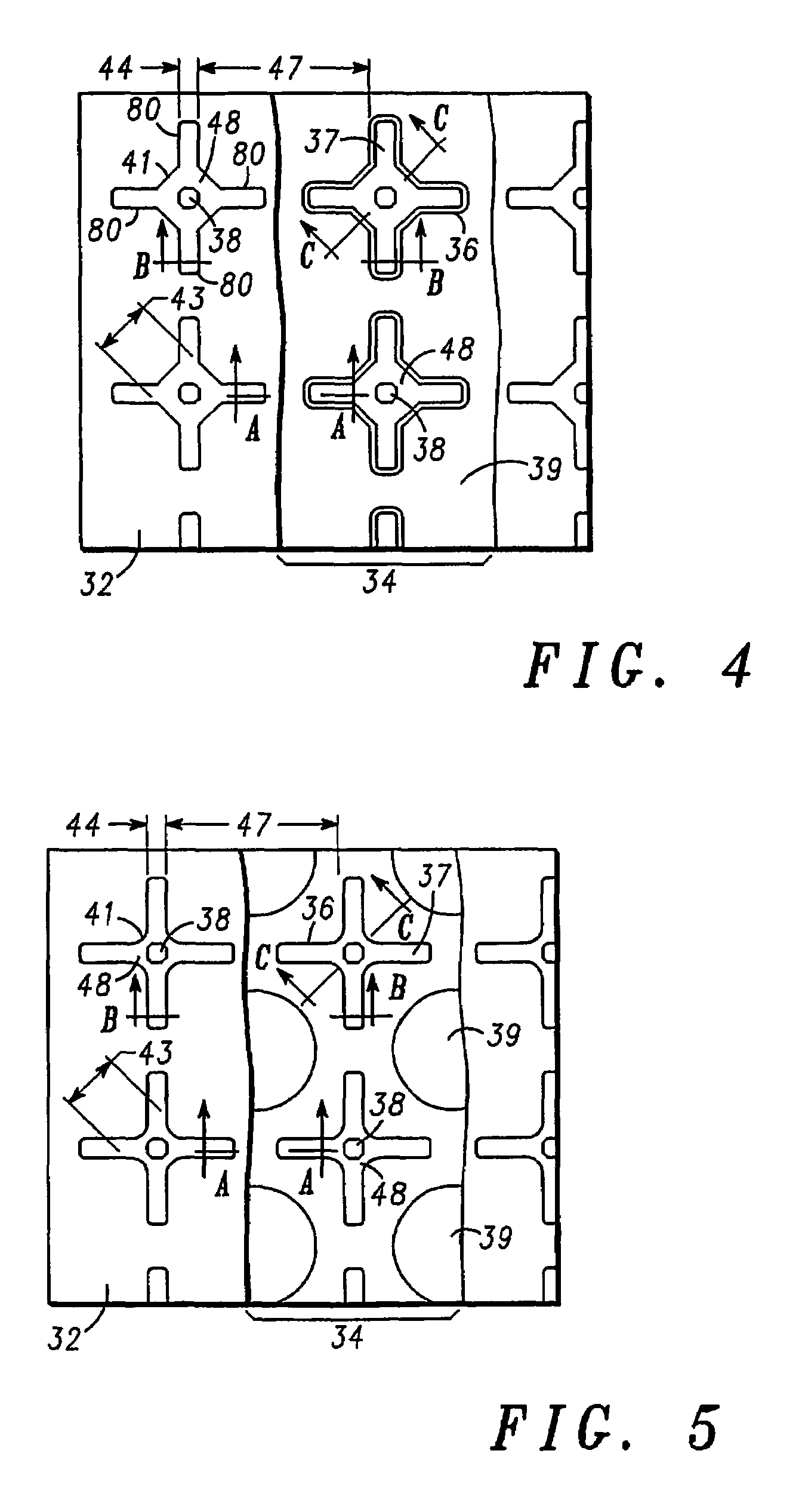
[0037]FIG. 4 depicts in more detail a top view of individual cells with four branches arranged crosswise of a semiconductor device according to an embodiment of the present invention before the merge operation. This arrangement aims at having improved channel density and low on-state resistance.

[0038]As is shown in FIG. 4, each individual cell has two horizontal branches and two vertical branches. The four branches of each individual cell are arranged so...


PUM


Abstract

A low on-state resistance power semiconductor device has a shape and an arrangement that increase the channel density and the breakdown voltage The power semiconductor device comprises a plurality of individual cells formed on a semiconductor substrate (62). Each individual cell comprises a plurality of radially extending branches (80) having source regions (37) within base regions (36). The plurality of individual cells are arranged such that at least one branch of each cell extends towards at least one branch of an adjacent cell and wherein the base region (36) of the extending branches merge together to form a single and substantially uniformly doped base region (36) surrounding drain islands (39) at the surface of the semiconductor substrate (62).

Description

FIELD OF THE INVENTION[0001]The invention relates, in general, to semiconductor processing techniques and more particularly to a power semiconductor device with a single continuous base region and method therefor.BACKGROUND OF THE INVENTION[0002]Semiconductor devices such as MOSFETs (Metal Oxide Semiconductor Field Effect Transistors) have been used in power electronics applications due to their appreciable current carrying and off-state voltage blocking capability with low on-state voltage drop. In terms of industrial applications, Power MOSFET devices are commonly used in many electronics fields such as portable electronics, power supplies, telecommunications and more particularly in many industrial applications relating to automotive electronics.[0003]Conventionally, a power MOSFET has a vertical oriented four-layer structure of alternating p-type and n-type doping. For instance, the n+pn-n+ structure is termed enhancement mode n-channel MOSFET. By applying a voltage higher than ...

Claims


Application Information

Patent Timeline
Patent Type & Authority Patents(United States)
IPC IPC(8): H01L21/337H01L29/06H01L29/78
CPCH01L29/0696H01L29/7802
Inventor REYNES, JEAN-MICHELDERAM, IVANAFEYBESSE, ADELINE
Owner NXP USA INC
Why Eureka
Try Eureka