Plasma display panel and method for manufacturing same

a technology of plasma display panel and manufacturing method, which is applied in the manufacture of electric discharge tubes/lamps, television systems, electrode systems, etc., can solve the problems of easy discharge-to-discharge variability between discharge cells, easy to increase the cost of pdps, and difficult to achieve satisfactory image display performance. , to achieve the effect of suppressing discharge variability, good secondary electron emission properties, and reducing firing voltage v

Inactive Publication Date: 2008-10-07
PANASONIC CORP
View PDF37 Cites 12 Cited by
  • Summary
  • Abstract
  • Description
  • Claims
  • Application Information

AI Technical Summary

Benefits of technology

[0017]That is, an electric field generated in the discharge space when the PDP is driven excites the discharge gas, causing rare gas atoms in the discharge gas to move toward the surface of the protective layer. This initiates the so-called Auger process according to which electrons in a valence band of the protective layer migrate, causing other electrons in the protective layer to be ejected by potential emission (PE) into the discharge space. Very good secondary electron emission properties are exhibited as a result, allowing the firing voltage Vf to be reduced. This potential emission thus enables the protective layer to achieve a required level of secondary electron emission (y) despite the electron emission properties of the MgO crystal being only moderate. Adequate effects are thus obtained even when a low cost MgO precursor used when forming the protective layer by a thick film technique is employed in the MgO crystal of the present invention.
[0018]The properties of the protective layer related to suppressing discharge variability are exhibited by the fine MgO crystalline particles, whose very pure crystal structure results in excellent electron emission properties. That is, when the electric field is generated in the discharge space, firstly the electrons in the fine MgO crystalline particles migrate to oxygen deficient regions as a result of the vacuum ultraviolet (VUV) that accompanies the electric field. The oxygen deficient regions then act as the luminescence center due to the energy difference between the electrons in these regions, and emit visible light. The visible light causes electrons in the fine MgO crystalline particles to be excited from the valence band to an energy level in a vicinity of the conduction band. The carrier density of the protective layer is improved by this increase in impurity electrons, allowing for impedance control. The occurrence of black noise is thus prevented in addition to any discharge-to-discharge variability when the PDP is driven being controlled and discharge probability improved, enabling very good image display properties to be exhibited.

Problems solved by technology

A high voltage transistor is thus needed in the drive IC, this being one of the factors hiking up the cost of PDPs.
However, with protective layers formed using a thick film technique, discharge-to-discharge variability between the discharge cells readily occurs when the PDP is driven, despite there being only slight gains in reduced firing voltage Vf over protective layers formed by thin film techniques using a vacuum process.
Discharge variability is a problem that needs addressing since it results in so-called “black noise”, possibly making it difficult to achieve satisfactory image display performance.
Black noise is when selected discharge cells fail to turn ON, increasing the likelihood of a demarcation arising between illuminated and non-illuminated areas on the screen.

Method used


Image

  • Plasma display panel and method for manufacturing same
  • Plasma display panel and method for manufacturing same
  • Plasma display panel and method for manufacturing same

Examples


embodiment 1

1-1. PDP Structure

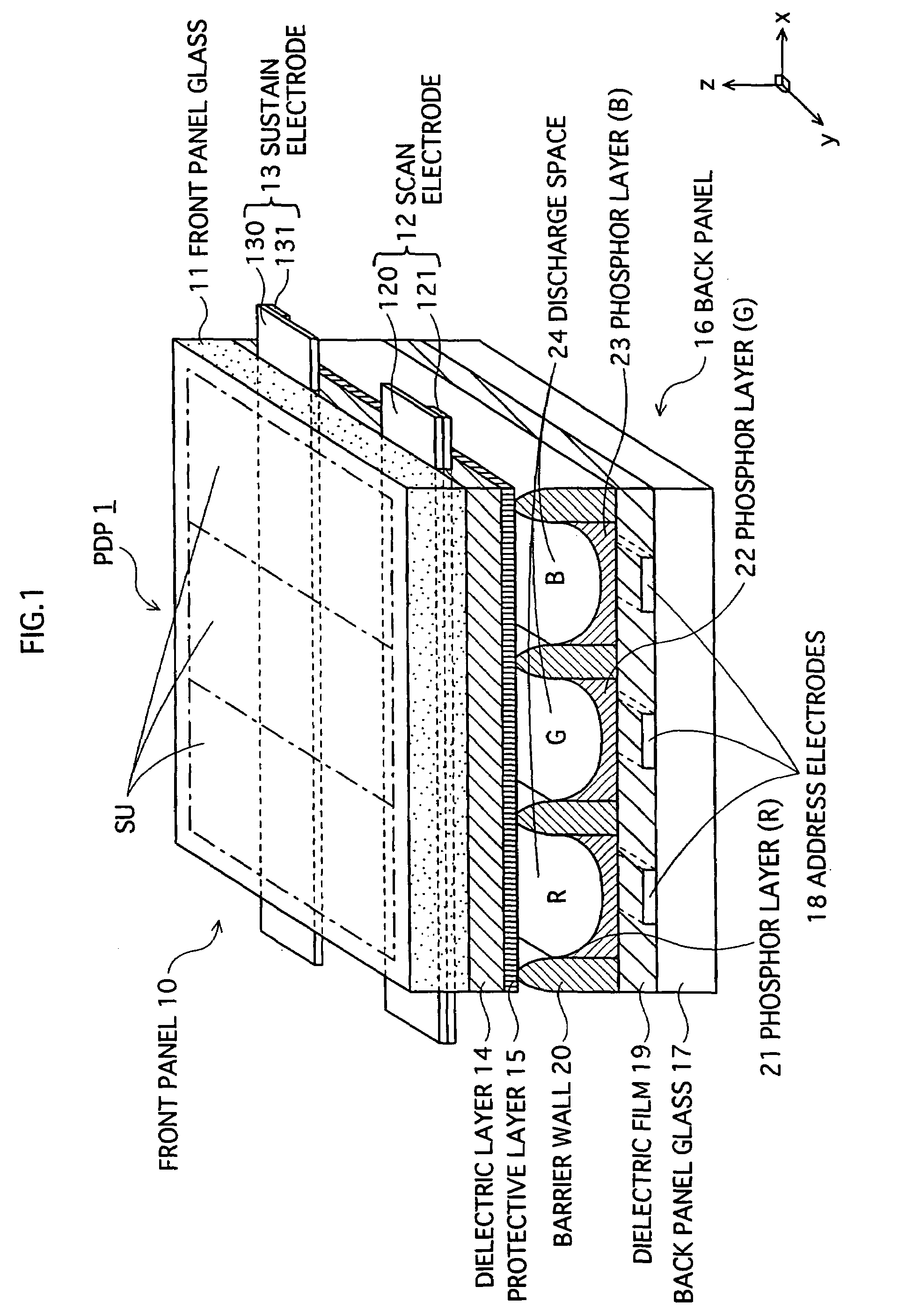
[0029]FIG. 1 is a partial sectional view showing the main structure of an AC PDP 1 in embodiment 1 of the present invention. In FIG. 1, the z direction corresponds to a thickness direction of PDP 1, and the xy direction corresponds to a plane parallel with the panel surfaces of PDP 1. In the example given here PDP 1 is a 42-inch class PDP conforming to NTSC specifications, although the present invention may naturally be applied to other sizes and specifications such as XGA, SXGA and the like.

[0030]As shown in FIG. 1, PDP 1 is broadly divided into a front panel 10 and a back panel 16 disposed with main surfaces opposing each other.

[0031]Plural pairs of display electrodes 12 and 13 (scan electrodes 12, sustain electrodes 13) are disposed on a main surface of a front glass panel 11 forming a substrate of front panel 10. Display electrodes 12 and 13 are formed by respectively layering buslines 121 and 131 (thickness: 7 μm; width: 95 μm) made from a silver (Ag) thick fi...

embodiment 2

3. Embodiment 2

[0088]The structure of a PDP of embodiment 2 is described next using FIG. 4.

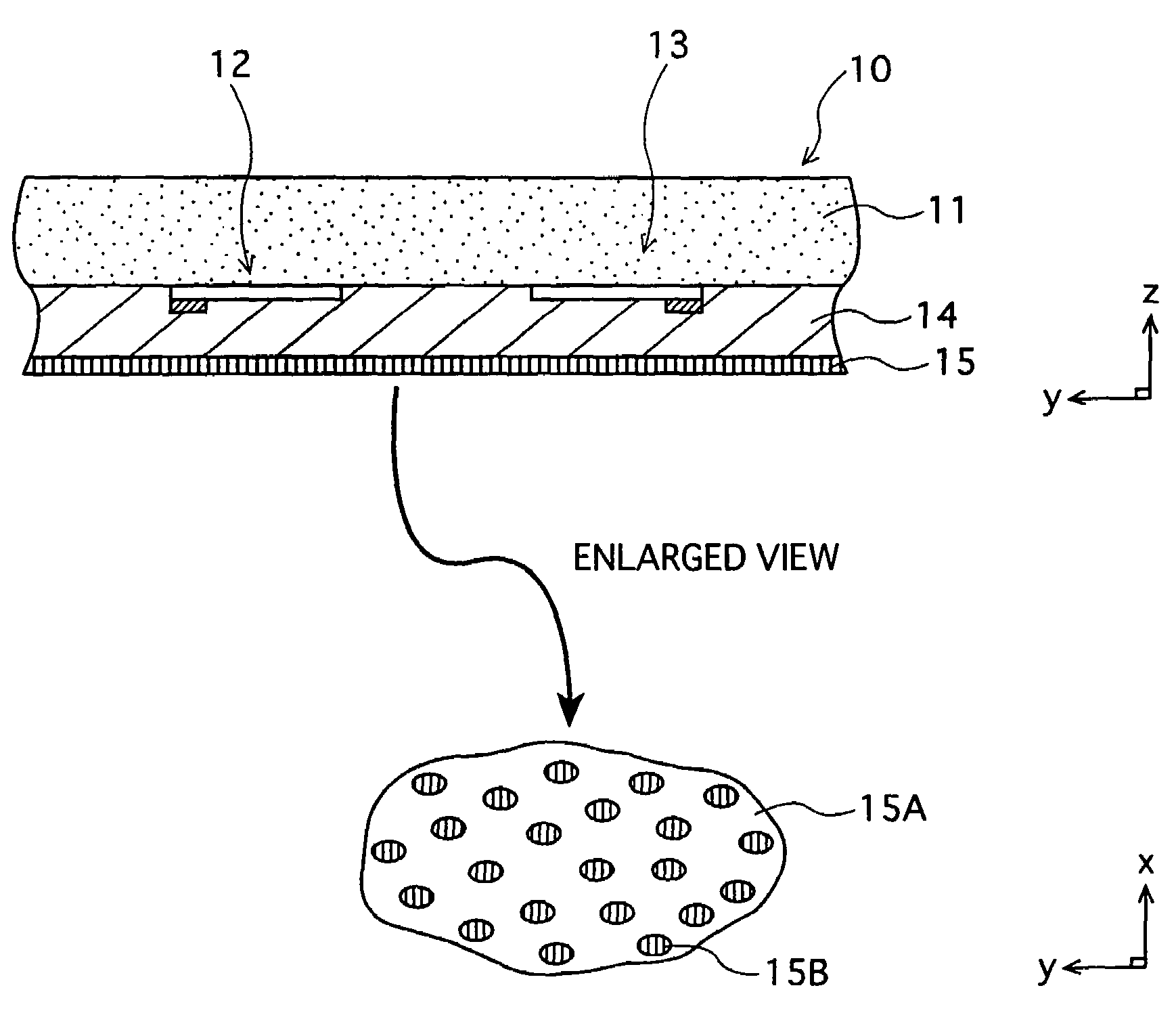
[0089]Instead of fine MgO crystalline particles 15B, protective layer 15 of embodiment 2 has carbon nanotubes (CNT) 15C formed from carbon crystal dispersed throughout MgO crystal 15A so as to be exposed to discharge spaces 24. MgO crystal 15A and CNT 15C are respectively assigned the tasks of reducing the firing voltage Vf and controlling discharge variability required of protective layer 15. Protective layer 15 can, for example, be formed by adding CNT to an organic material that includes an MgO precursor, applying the organic material with additive CNT to the front panel, and baking the applied material.

[0090]With a PDP having the above structure, MgO crystal 15A exhibits the same effects as embodiment 1 when the PDP is driven. The excellent emission properties of CNT 15C allow for the secondary electron emission coefficient (Υ) of protective layer 15 as well as MgO crystal 15A to be improv...

embodiment 3

5. Embodiment 3

5-1. Structure of Protective Layer

[0094]PDP 1 of an embodiment 3 is described next using the partial cross-sectional views of the PDP shown in FIGS. 6A and 6B.

[0095]FIG. 6A is a cross-sectional view in the x direction, while FIG. 6B is a cross-sectional view in the y direction that cuts FIG. 6A at a-a′. The basic structure of PDP 1 is similar to embodiments 1 and 2, with a difference lying only in the structure of protective layer 15, which is a feature of the present invention.

[0096]In PDP 1 of embodiment 3, as shown in FIGS. 6A and 6B, at least a surface of protective layer 15 is structured from a base made from MgO as a first material and isolated metal parts 150 made from a metal material having a higher Fermi energy than the MgO of the base as a second material, the isolated metal parts being deposited on the base so as to face into discharge spaces 24. Specifically, isolated metal parts 150 are positioned so as to overlap in the thickness direction of the panel ...


PUM

PropertyMeasurementUnit
sizeaaaaaaaaaa
thicknessaaaaaaaaaa
thicknessaaaaaaaaaa

Abstract

A plasma display panel in which a first substrate having a protective layer formed thereon opposes a second substrate across a discharge space, with the substrates being sealed around a perimeter thereof. At a surface of the protective layer, first and second materials of different electron emission properties are exposed to the discharge space, with at least one of the materials existing in a dispersed state. The first and second materials may be first and second crystals, and the second crystal may be dispersed throughout the first crystal.

Description

TECHNICAL FIELD[0001]The present invention relates to manufacturing methods for gas discharge panels such as plasma display panels, and in particular to improving the protective layer.BACKGROUND ART[0002]A plasma display panel (PDP) is a type of gas discharge panel that achieves image display by using UV light from gas discharges to excite phosphors to emit visible light. PDPs can be classified into alternating current (AC) and direct current (DC) types on the basis of how discharges are formed, with the AC type being more typical because of its superiority in terms of luminance, luminous efficiency and device life.[0003]In an AC PDP, two thin glass panel surfaces having a plurality of electrodes (display & address electrodes) disposed thereon and dielectric layers covering the electrodes oppose each other via a plurality of barrier ribs. Phosphor layers are disposed between adjacent barrier ribs and a discharge gas is enclosed between the two glass panels, with a plurality of disch...

Claims


Application Information

Patent Timeline
Patent Type & Authority Patents(United States)
IPC IPC(8): H01J5/06H01J9/02H01J11/12H01J11/22H01J11/24H01J11/26H01J11/34H01J11/40
CPCH01J9/02H01J11/40H01J11/12
Inventor MORITA, YUKIHIROKITAGAWA, MASATOSHIOISHI, KIICHIRONISHITANI, MIKIHIKO
Owner PANASONIC CORP
Why Eureka
Try Eureka