Semiconductor device reducing power consumption in standby mode

a technology of semiconductor devices and power consumption, applied in power consumption reduction, pulse techniques, instruments, etc., can solve the problems of power consumption increase in transistors pb>2/, storage information may be lost, semiconductor devices cannot be restored to the original state, etc., and achieve the effect of reducing power consumption

Inactive Publication Date: 2008-10-14
RENESAS ELECTRONICS CORP
View PDF10 Cites 46 Cited by
  • Summary
  • Abstract
  • Description
  • Claims
  • Application Information

AI Technical Summary

Benefits of technology

[0026]The invention has been made for overcoming the above problems, and it is an object of the invention to provide a semiconductor device that can reduce power consumption.
[0028]The semiconductor device according to the invention includes the internal circuit forming the current path between the second voltage interconnection and the first voltage supply interconnection; and the first voltage supply control circuit capable of controlling the state of electrical conduction between the first voltage supply interconnection and the first voltage interconnection. The first voltage supply control circuit includes the first switch arranged between the first voltage supply interconnection and the first voltage interconnection, the second switch arranged between the third voltage interconnection and the control end of the first switch, and electrically coupling the third voltage interconnection to the control end of the first switch according to the instruction signal turning on the first switch, and the third switch electrically coupling the first voltage supply interconnection to the control end of the first switch according to the instruction signal attaining the off state of passing a smaller quantity of current through the first switch than the on state. When the first switch is turned on according to the instruction signal, the control end of the first switch is charged by a third voltage. When the first switch is turned off according to the instruction signal, the third switch electrically couples the first voltage supply interconnection to the control end of the first switch to discharge the charges. Thereby, the current path of the internal circuit arranged between the first and second voltage interconnections can reduce the quantity of charges pulled out from the second voltage interconnection, and thereby can reduce the power consumption. Since the third switch is connected to the first voltage interconnection through the first switch, a current interrupting effect of the first switch can reduce the leak current leaking to the first voltage interconnection via the third switch. Therefore, the leak current of the first voltage supply control circuit can be reduced, and the current consumption of the whole circuit can be reduced.

Problems solved by technology

Thus, the power consumption increases in transistors P2 and Q1.
Thus, stored information may be lost.
Consequently, the semiconductor device cannot be restored to the original state even when it enters an active mode after the standby period.

Method used


Image

  • Semiconductor device reducing power consumption in standby mode
  • Semiconductor device reducing power consumption in standby mode
  • Semiconductor device reducing power consumption in standby mode

Examples


first embodiment

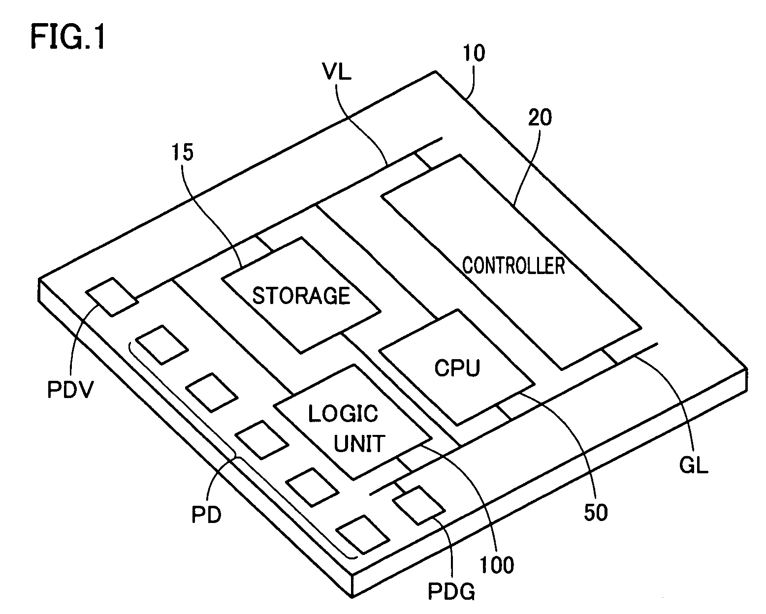
[0063]Referring to FIG. 1, a semiconductor device 10 according to a first embodiment of the invention includes a CPU 50 controlling a whole circuit, a storage 15 having a memory for storing information, a controller 20 that is a peripheral circuit for producing a clock signal or a control signal, and a logic unit 100 for executing various arithmetic and logic operations.

[0064]In general, the semiconductor device is provided at its peripheral region with pads, and is supplied via the pads with, e.g., a power supply voltage, a ground voltage, external instruction signals and the like. In this example, FIG. 1 shows a power supply voltage pad PDV supplied with a power supply voltage Vcc, a ground voltage pad PDG supplied with a ground voltage GND and pads PD supplied with other voltages, external instruction signals and the like.

[0065]FIG. 1 shows, by way of example, a ground line GL for supplying the ground voltage for the circuits via ground voltage pad PDG. There is also arranged a p...

second embodiment

[0226]In the foregoing first embodiment, an example of the internal circuit included in semiconductor device 10 has been described on the manner of reducing the power consumption in the standby mode, using the voltage supply control circuit for logic circuit group L1 included in logic unit 100. In contrast to this, the second embodiment will be described in connection with a structure applied for reducing the power consumption of memory cells MC in a storage, which is an example of the internal circuit.

[0227]Referring to FIG. 22, a part of a storage 15 according to the second embodiment of the invention will now be described.

[0228]Referring to FIG. 22, storage 15 according to the second embodiment of the invention includes a memory array MA including memory cells MC arranged in rows and columns, a row decoder 62 selecting rows of memory cells MC, a column decoder 66 selecting a column of memory cells MC, a control circuit 63 such as row and column decoders for controlling circuit bl...

third embodiment

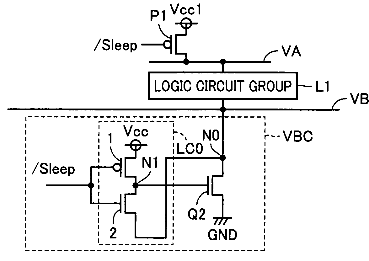
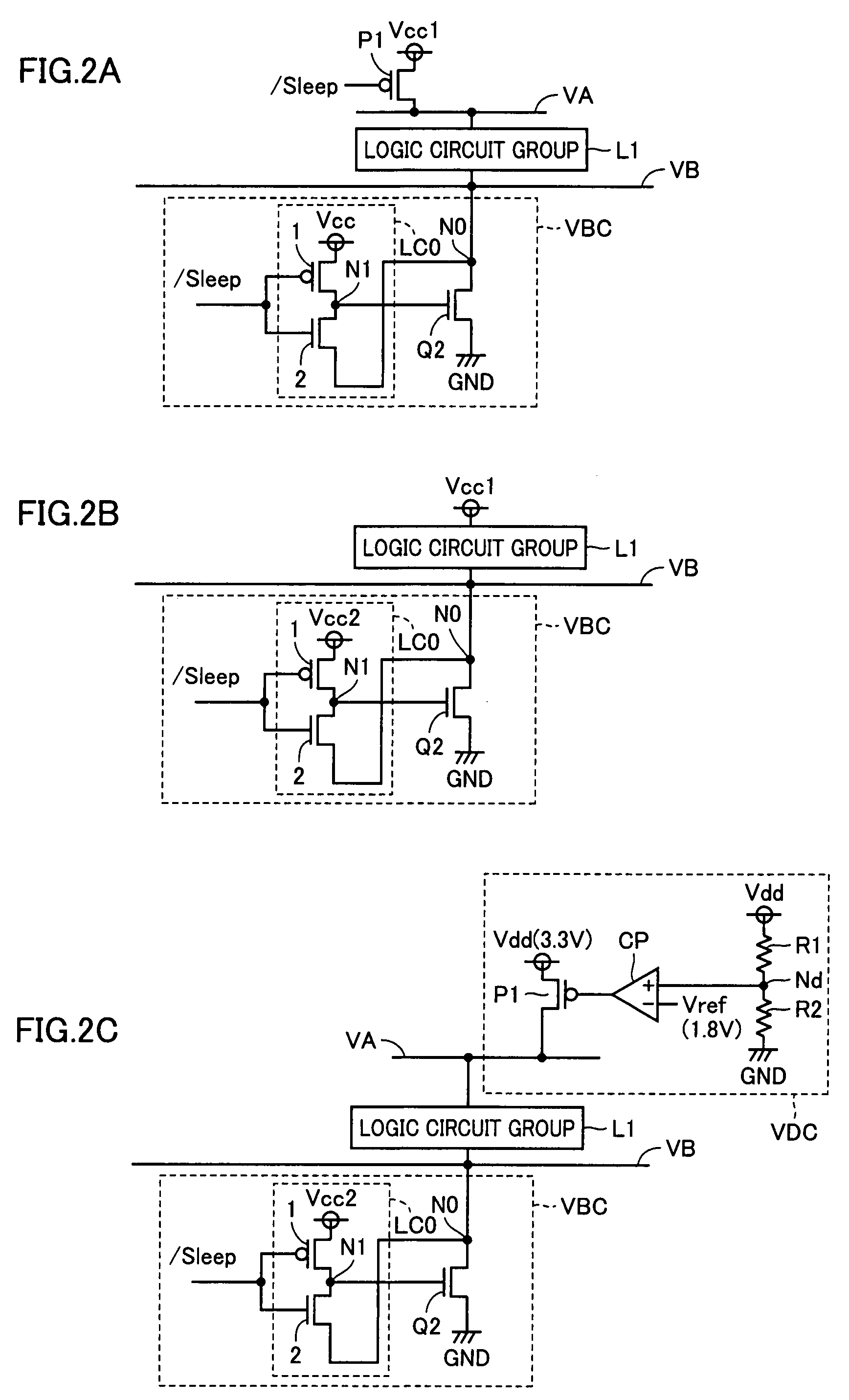
[0290]In the description described above, two transistors operate complementarily to each other to control the voltage level of pseudo ground line VB in response to control signal / Sleep, for example, as is done in voltage supply control circuit VBC in FIGS. 2A-2C. However, this is not restrictive, and such a manner may be employed that the transistors receive independent control signals for operations, respectively.

[0291]FIGS. 33A and 33B illustrate an MTCMOS circuit according to a third embodiment of the invention.

[0292]Referring to FIG. 33A, voltage supply control circuit VBC already described is replaced with voltage supply control circuit VBC#p. Voltage supply control circuit VBC#p includes three switches SW1-SW3.

[0293]Switch SW1 is arranged between node N0 and ground voltage GND, and receives a voltage signal from node N1. Switch SW2 is arranged between node N1 and power supply voltage Vcc, and receives a control signal Sleep2. Switch SW3 is arranged between nodes N1 and N0, a...


PUM


Abstract

A voltage supply control circuit is arranged between a true ground voltage and a pseudo ground line. In an active mode, first and second control signals are at the “H” and “L” levels, respectively. In response to this, a first switch is turned on so that a first node is electrically coupled to a power supply voltage, and attains the “H” level. Further, a second switch is turned on to couple electrically the ground voltage to a second node. In a standby mode, the first and second control signals are at the “L” and “H” levels, respectively. In response to this, a third switch is turned on to couple electrically the first and second nodes together. Since the power supply voltage was electrically coupled to the first node according to the turn-on of the first switch in the active mode, the path of the control signal including the first node to the switch has accumulated charged charges.

Description

BACKGROUND OF THE INVENTION[0001]1. Field of the Invention[0002]The present invention relates to a semiconductor device. Particularly, the invention relates to a semiconductor device having a structure that interrupts electric connections of power and ground lines to logic circuits or the like in a standby mode, and is pertinent to a semiconductor device that can reduce power consumption in the standby mode.[0003]2. Description of the Background Art[0004]In recent years, degrees of integration as well as performance of semiconductor devices have been developing, and application ranges thereof have been increasing. With these situations, it has been technically required to reduce power consumption of semiconductor devices and semiconductor chip bodies. More specifically, it is required to increase a battery operation time of an internal battery in a data information device that includes a telephone, an electronic notebook and a small personal computer in an integrated fashion. In inf...

Claims


Application Information

Patent Timeline
Patent Type & Authority Patents(United States)
IPC IPC(8): H03K17/16
CPCH03K19/0016G11C11/417
Inventor TADA, AKIRA
Owner RENESAS ELECTRONICS CORP
Why Eureka
Try Eureka