

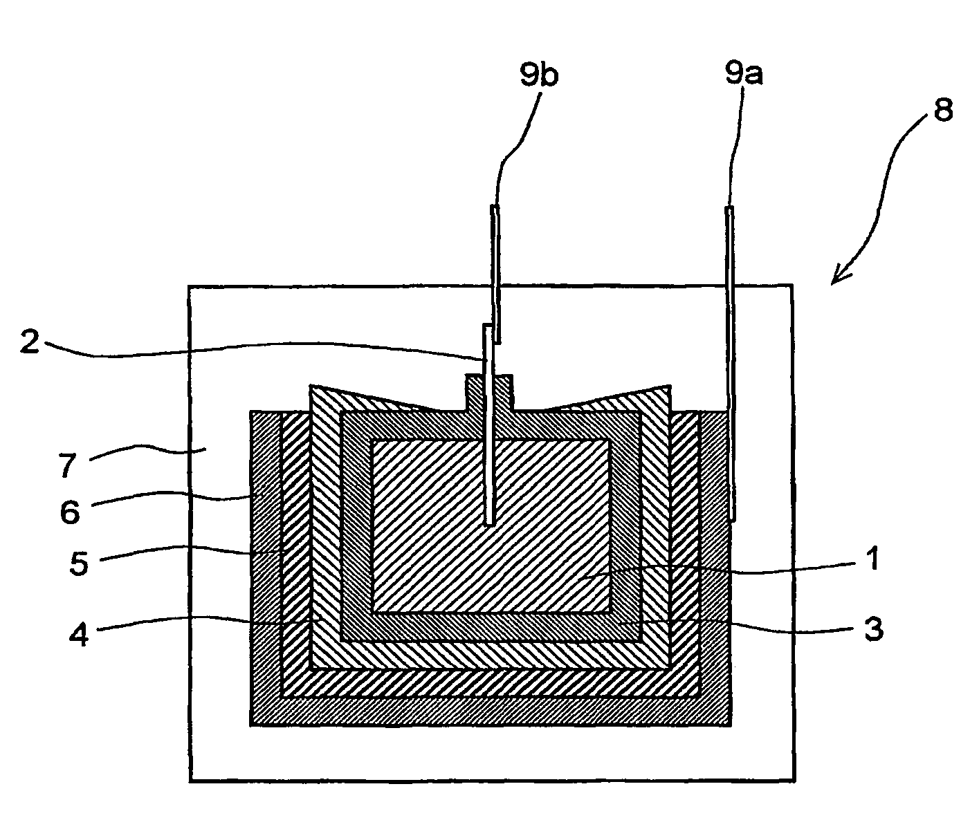
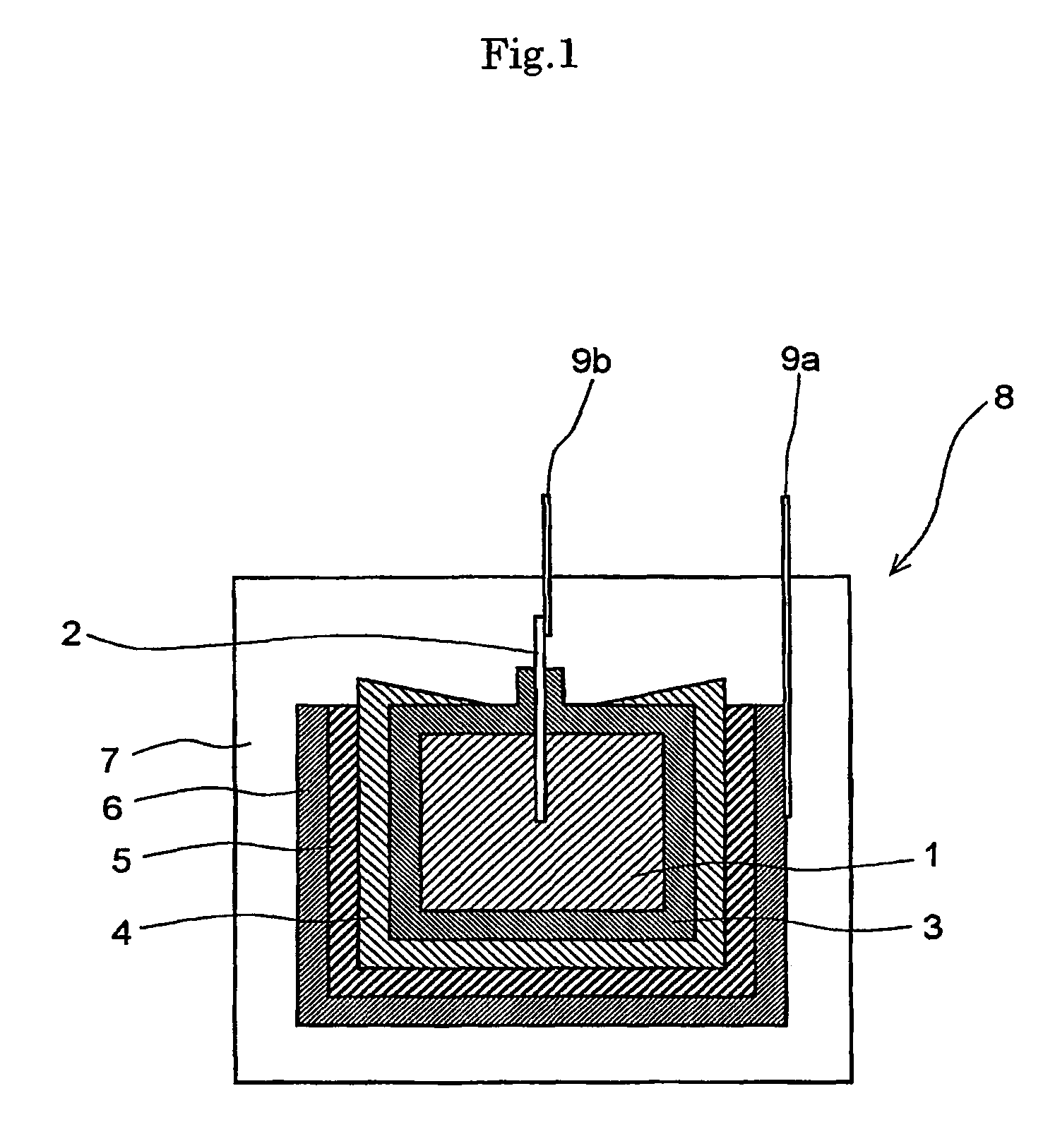
Solid electrolyte capacitor
a solid electrolyte capacitor and capacitor technology, applied in the direction of electrolytic capacitors, capacitor electrodes, liquid electrolytic capacitors, etc., can solve the problems of difficulty in reducing the lc value by conventional techniques such as re-electrochemical formation, aging, or even by, and achieve good electrical contact and high lc value
- Summary
- Abstract
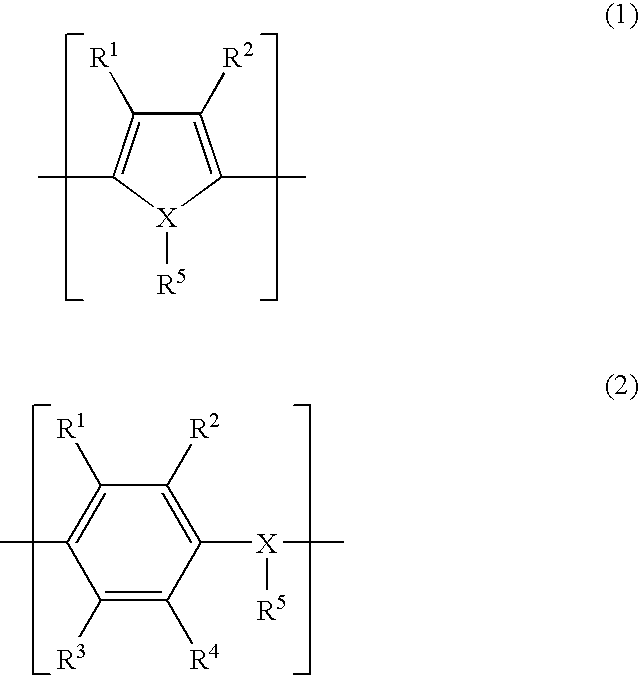
- Description
- Claims
- Application Information
AI Technical Summary
Benefits of technology
Problems solved by technology
Method used
Image

Examples
example 1
[0077]By using and shaping a niobium powder having CV (product of capacitance and electrochemical voltage) of 200,000 μF·V / g together with a niobium lead wire of 0.29 mmφ, a sintered body in a size of 4.5×3.0×1.0 mm was produced (nitrided amount of the powder: 11,000 ppm, amount of oxygen due to natural oxidation on the powder surface: 80,000 ppm, sintering temperature: 1,270° C., sintering time: 30 minutes, density of sintered body: 3.6 g / cm3, an Nb lead wire was vertically implanted in the center part of the 1.0×3.0 mm face of the sintered body while implanting the lead 4 mm deep inside the sintered body with 10 mm of the lead protruding outside the sintered body). The lead wires having the same dimension of 32 sintered bodies prepared above were arrayed and connected at regular intervals on a separately prepared stainless steel-made long metal plate having a length of 250 mm, a width of 20 mm and a thickness of 2 mm while leaving the 30 mm margins unused in the right and left edg...
example 2
[0080]A chip solid electrolyte capacitor where the thickness of the semiconductor layer in the vicinity of the lead wire-implanted part was 2 μm was produced in the same manner as in Example 1 except that the formation of fine deposits was conducted on the surface including the face implanted with the lead wire and that out of the 15 repetitions of the step for forming the semiconductor layer, 5 repetitions were performed on the whole surface of the sintered body including the face implanted with the lead wire.
example 3
[0081]A chip solid electrolyte capacitor where the thickness of the semiconductor layer in the vicinity of the lead wire-implanted part was 5 μm was produced in the same manner as in Example 1 except that the formation of fine deposits was conducted also on the face implanted with the lead wire and that out of the repetitions of the step for forming the semiconductor layer, 7 repetitions were performed on the whole surface of the sintered body including the face implanted with the lead wire.
PUM
| Property | Measurement | Unit |
|---|---|---|
| thickness | aaaaa | aaaaa |
| thickness | aaaaa | aaaaa |
| thickness | aaaaa | aaaaa |
Abstract
Description
Claims
Application Information