Image processing device and method

a processing device and image technology, applied in the field of image processing apparatus and method, can solve the problems of heavy scene data analysis load, inability to achieve parallel property, and fast technological advances in graphic lsis, and achieve the effect of reducing the size of the crossbar circuit and increasing the processing speed

Inactive Publication Date: 2008-10-14
SONY CORP
View PDF18 Cites 12 Cited by
  • Summary
  • Abstract
  • Description
  • Claims
  • Application Information

AI Technical Summary

Benefits of technology

[0034]An object of the present invention is to provide an image processing apparatus and method thereof that can achieve a reduction in the size of a crossbar circuit and achieve an increase in speed of processing.

Problems solved by technology

Further, the technological advances being made in graphic LSIs have been fast.
In the case of parallel processing by area division explained above, however, in order to make the processing units operate in parallel efficiently, it is necessary to classify objects to be drawn in the areas in advance, so the load of the scene data analysis is heavy.
Further, when not starting drawing after one frame's worth of the scene data is all present, but drawing in the so-called immediate mode of starting drawing immediately when object data is given, the parallel property cannot be achieved.
When this difference becomes large, the areas which the processing units draw in also largely differ and the locality of the data is lost, so for example the DRAM comprising the memory modules frequently makes page errors and the performance is lowered.
Further, in the case of this technique, there is also the problem of a high interconnect cost.
However, a related image processing apparatus, as described above, globally distributes data to the processing units, then performs texture filtering, so there are the disadvantages that the amount of data globally distributed is large (for example, 4 Tbps), the crossbar circuit serving as the global bus becomes large in size, and an increase in the speed of processing is obstructed from the viewpoint of interconnect delay etc.

Method used


Image

  • Image processing device and method
  • Image processing device and method
  • Image processing device and method

Examples


Embodiment Construction

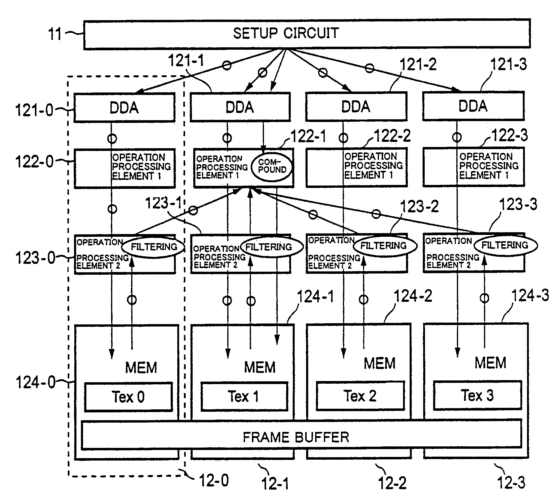
[0061]FIG. 4 is a block diagram of the configuration of an embodiment of an image processing apparatus according to the present invention.

[0062]An image processing apparatus 10 according to the present embodiment has, as shown in FIG. 4, a setup circuit 11, processing modules 12-0 to 12-3, and a crossbar circuit 13.

[0063]In the present image processing apparatus 10, a plurality of, four in the present embodiment, processing modules 12-0 to 12-3 are connected in parallel to a setup circuit 11. A plurality of processing modules 12-0 to 12-3 share processing data to perform parallel processing.

[0064]Then, for the texture read system, memory access to other processing modules is necessary, but a crossbar circuit 13 serving as a global access bus is used for this access.

[0065]Below, the configurations and functions of the components are described sequentially with reference to the drawings.

[0066]The setup circuit 11 controls the transfer of data with a CPU and an external memory and the ...


PUM


Abstract

An image processing apparatus and method which can achieve a reduction in size of the crossbar circuit and achieve a higher speed of processing, which perform DDA processing (ST11), then read out texture data from a memory (ST12), perform sub-word reallocation processing (ST13), then perform texture-filtering (ST14), then globally distribute data by the crossbar circuit 13 to a first operation processing element of each processing module (ST15), then perform processing at the pixel level, specifically use the texture data after filtering and the various types of data after rasterization to perform operations by pixel units and draw the pixel data passing the various types of tests in the processing at the pixel level to a frame buffer on a memory module (ST16).

Description

TECHNICAL FIELD[0001]The present invention relates to an image processing apparatus and method thereof wherein a plurality of processing devices share processing data to perform parallel processing.BACKGROUND ART[0002]In recent years, graphic LSIs for performing 3D computer graphics by hardware at a high speed have spread remarkably. In particular, in game systems and personal computers (PC), such graphic LSIs are often mounted as standard equipment.[0003]Further, the technological advances being made in graphic LSIs have been fast. Expansion of functions such as in the “Vertex Shader” and “Pixel Shader” employed in “DirectX” have been continuing and performance has been improved at a pace faster than that of the CPUs.[0004]In order to improve the performance of a graphic LSI, it is effective not only to raise the operating frequency of the LSI, but also to utilize the techniques of parallel processing. The techniques of parallel processing may be roughly classified as follows.[0005...

Claims


Application Information

Patent Timeline
Patent Type & Authority Patents(United States)
IPC IPC(8): G06K9/60G06F15/80G06K9/36G09G5/00G06F15/16G06F15/173G06F17/10G06T1/20G06T5/20
CPCG06T1/20G06T15/005G06T15/04G06F15/16G06F17/10G06T17/00
Inventor SATOH, JIN
Owner SONY CORP
Why Eureka
Try Eureka