Methods and batch type atomic layer deposition apparatus for forming dielectric films and methods of manufacturing metal-insulator-metal capacitors including the dielectric films

a technology of atomic layer deposition and dielectric film, which is applied in the direction of capacitors, chemical vapor deposition coatings, coatings, etc., can solve the problems of film thermal degradation, large leakage current, and low throughput, so as to reduce or prevent the leakage current of the dielectric film and improve the throughput of the device

Active Publication Date: 2008-10-28
SAMSUNG ELECTRONICS CO LTD
View PDF14 Cites 6 Cited by
  • Summary
  • Abstract
  • Description
  • Claims
  • Application Information

AI Technical Summary

Benefits of technology

[0008]The present invention provides methods of forming a dielectric film on larger caliber wafers, which can reduce or prevent leakage current of the dielectric film during a higher temperature process and improve the throughput of a device. The present invention also provides methods of manufacturing a metal-insulator-metal (MIM) capacitor using the methods of forming the dielectric film. The present invention further provides apparatus for forming the dielectric films.

Problems solved by technology

However, a capacitor having the TiN / HfO2 / TiN structure may generate a larger leakage current during a back-end process.
However, since a respective process may be performed for each wafer when the single type ALD apparatus is used, formation of dielectric films on several wafers may require additional time, resulting in a lower throughput.
However, when the Al2O3 film is deposited at about 250 to 350° C., the film may be thermally degraded such that a sufficiently high crystallization temperature of the Al2O3 film may not be obtained.
Therefore, the Al2O3 film may not increase the crystallization temperature of the capacitor dielectric film.
However, MIM capacitors formed on 300 mm large caliber wafers using conditions for forming MIM capacitors on 200 mm wafers may render it problematic to obtain optimized MIM capacitors.

Method used


Image

  • Methods and batch type atomic layer deposition apparatus for forming dielectric films and methods of manufacturing metal-insulator-metal capacitors including the dielectric films
  • Methods and batch type atomic layer deposition apparatus for forming dielectric films and methods of manufacturing metal-insulator-metal capacitors including the dielectric films
  • Methods and batch type atomic layer deposition apparatus for forming dielectric films and methods of manufacturing metal-insulator-metal capacitors including the dielectric films

Examples


example 1

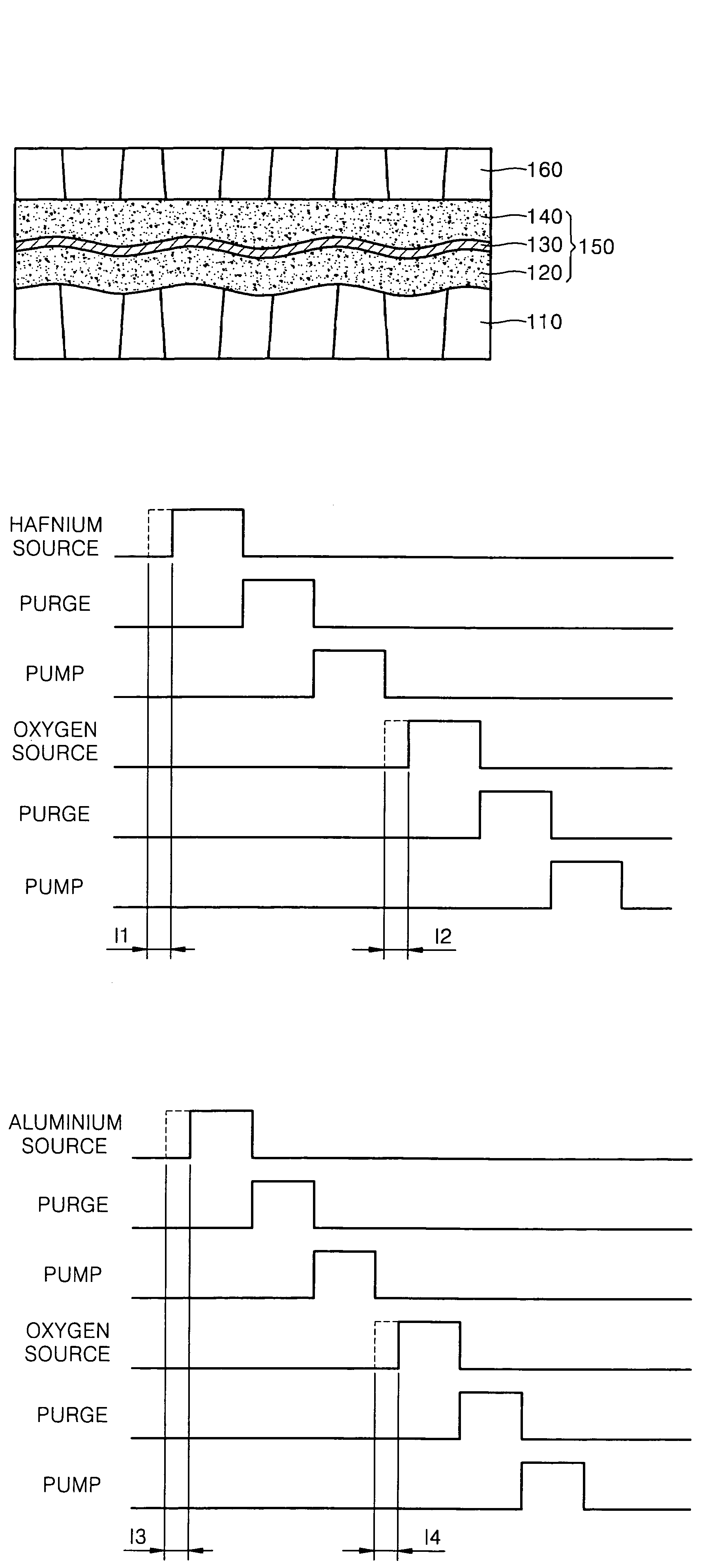
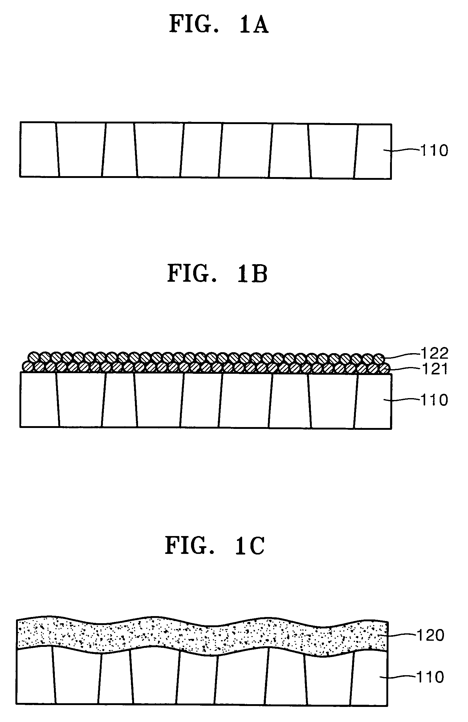
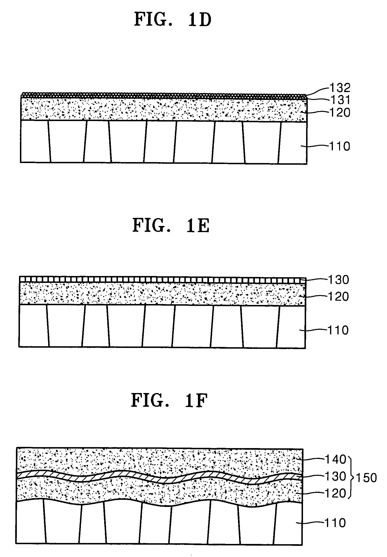
[0053]FIG. 6 presents a graph illustrating a degree of leakage current of a capacitor dielectric film according to some embodiments of the present invention in conjunction with results of a conventional capacitor dielectric film. In FIG. 6, the x-axis indicates capacitances (fF / cell) of the layers at −0.9V, and the y-axis indicates voltages corresponding to 1fA / cell. The leakage current can be estimated with a voltage corresponding to 1fA / cell. Reference symbols ● and ∘ in FIG. 6 indicate results when a first hafnium oxide layer 120 of about a 40Å thickness, an aluminum oxide layer 130 of about a 5Å thickness and a second hafnium oxide layer 140 of about a 40Å thickness are formed using the batch type ALD apparatus according to embodiments of the present invention, and reference symbols ★ and ⋆ in FIG. 6 indicate a first hafnium oxide layer 120 of about a 40Å thickness, an aluminum oxide layer 130 of about a 5 Å thickness, and a second hafnium oxide layer 140 of about a 40 Å thickne...

example 2

[0055]FIG. 7A presents a graph illustrating capacitances of a capacitor in which a dielectric film is formed using the batch type ALD apparatus according to some embodiments of the present invention in conjunction with capacitances of capacitors in which dielectric films are formed using a conventional single type ALD apparatus. FIG. 7B presents a graph illustrating breakdown voltages of the capacitor in which the dielectric film is formed using the batch type ALD apparatus according to embodiments of the present invention in conjunction with breakdown voltages of the capacitors in which dielectric films are formed using a conventional single type ALD apparatus.

[0056]Referring to FIG. 7A, the capacitances of the capacitor in which the dielectric film is formed using the batch type ALD apparatus according to some embodiments of the present invention and the capacitors in which dielectric films are formed using a conventional single type ALD apparatus are about 20 through 23 fF / cell.

[...


PUM

PropertyMeasurementUnit
temperatureaaaaaaaaaa

Abstract

Provided are methods of manufacturing dielectric films including forming a first dielectric film on a wafer using atomic layer deposition (ALD) in a first batch type apparatus, forming a second dielectric film on the first dielectric film using atomic layer deposition in a second batch type apparatus, wherein the second dielectric film has a higher crystallization temperature than the first dielectric film and forming a third dielectric film on the second dielectric film using atomic layer deposition in a third batch type apparatus. Methods of manufacturing metal-insulator-metal (MIM) capacitors using the methods of forming the dielectric films and batch type atomic layer deposition apparatus for forming the dielectric films are also provided.

Description

CROSS-REFERENCE TO RELATED APPLICATION[0001]This application claims the benefit of Korean Patent Application Nos. 10-2005-0024071, filed Mar. 23, 2005, and 10-2005-0069664, filed Jul. 29, 2005. The disclosures of these applications are incorporated herein by reference in their entirety as if fully set forth herein.FIELD OF THE INVENTION[0002]The present invention relates to methods and batch type atomic layer deposition (ALD) apparatus for forming dielectric films and methods of manufacturing metal-insulator-metal (MIM) capacitors including the dielectric films.BACKGROUND OF THE INVENTION[0003]A structure including titanium nitride film / hafnium oxide film / titanium nitride film (TiN / HfO2 / TiN) has been suggested for formation of a capacitor having a reduced leakage current and an increased capacitance. Since a capacitor including a TiN / HfO2 / TiN structure may be less expensive and may further possess a lower current density than a structure including ruthenium film / tantalum oxide film / ...

Claims


Application Information

Patent Timeline
Patent Type & Authority Patents(United States)
IPC IPC(8): H01L21/8242
CPCC23C16/45529C23C16/45546H01L21/3141H01L21/3142H01L28/56H01L21/31616H01L21/31645H01L21/0228H01L21/022H01L21/02205H01L21/02175H01L21/20H10B12/00
Inventor CHOI, JAE-HYOUNGCHUNG, JUNG-HEEOH, SE-HOONLEE, JONG-CHEOL
Owner SAMSUNG ELECTRONICS CO LTD
Why Eureka
Try Eureka