Multi-stage multiplexing chip set having switchable forward/reverse clock relationship

a multi-stage multiplexing and clock relationship technology, applied in the field of high-speed serial bit stream multiplexing, can solve the problems of high manufacturing cost, low effective yield of indium-phosphate or silicon-germanium process, and difficult data conversion. , to achieve the effect of slowing down the switching circuit and avoiding the use of costly processes

Active Publication Date: 2008-10-28
AVAGO TECH INT SALES PTE LTD
View PDF6 Cites 2 Cited by
  • Summary
  • Abstract
  • Description
  • Claims
  • Application Information

AI Technical Summary

Benefits of technology

[0014]The present invention provides a multistage bit stream multiplexer that couples a communication Application Specific Integrate Circuit (ASIC) to a high-speed bit stream media. More specifically, the present invention provides a multistage bit stream multiplexer having a switchable forward / reverse clock relationship. The multistage bit stream multiplexer includes a first multiplexing circuit that receives a first set of bit streams at a first bit rate and that produces a second set of bit streams at a second bit rate. The first set of bit streams are greater in number than the second set of bit streams are in number, and the first bit rate is less than the second bit rate. A second multiplexing circuit receives the second set of bit streams and outputs high-speed bit stream(s) at a bit rate that exceeds the second bit rate. The first and second multiplexing circuits may be formed on any combination of InP, SiGe, GaN, GaAs, or Si substrates. This staging of the multiplexing process allows the relatively slower switching circuits to employ standard processing techniques, while faster switching circuits that employ more costly processes may be simplified.

Problems solved by technology

Particular difficulties arise in converting data between the 40×1 GBPS line interface and the 16×2.5 GBPS communication ASIC interface.
While other materials, e.g., Indium-Phosphate and Silicon-Germanium provide higher switching rates than do Silicon based devices, they are very expensive and difficult to manufacture.
Thus, even if a device were manufactured that could perform such interfacing operations, the effective yield in an Indium-Phosphate or Silicon-Germanium process would be very low.
While this choice permits the upstream circuit to be simpler, there also can be problems associated with generating the clock on the chip that is receiving the data, such as jitter and phase alignment issues.

Method used


Image

  • Multi-stage multiplexing chip set having switchable forward/reverse clock relationship
  • Multi-stage multiplexing chip set having switchable forward/reverse clock relationship
  • Multi-stage multiplexing chip set having switchable forward/reverse clock relationship

Examples


Embodiment Construction

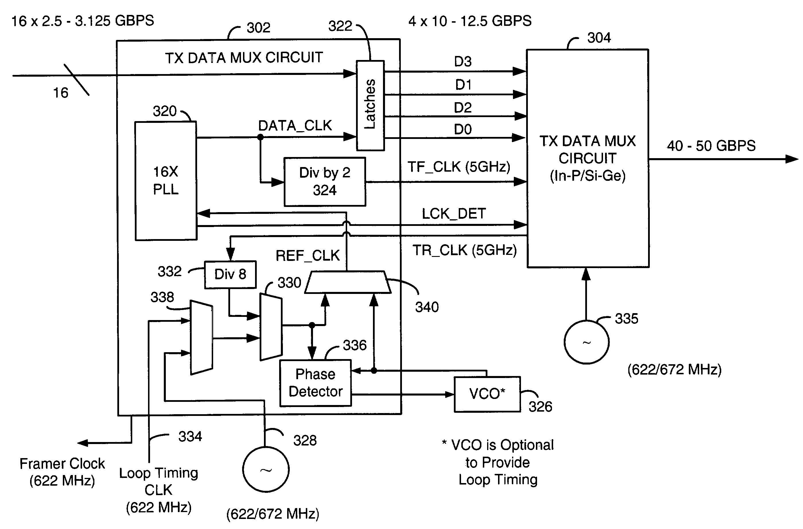
[0043]Preferred embodiments of the present invention are illustrated in the FIGUREs, like numerals being used to refer to like and corresponding parts of the various drawings.

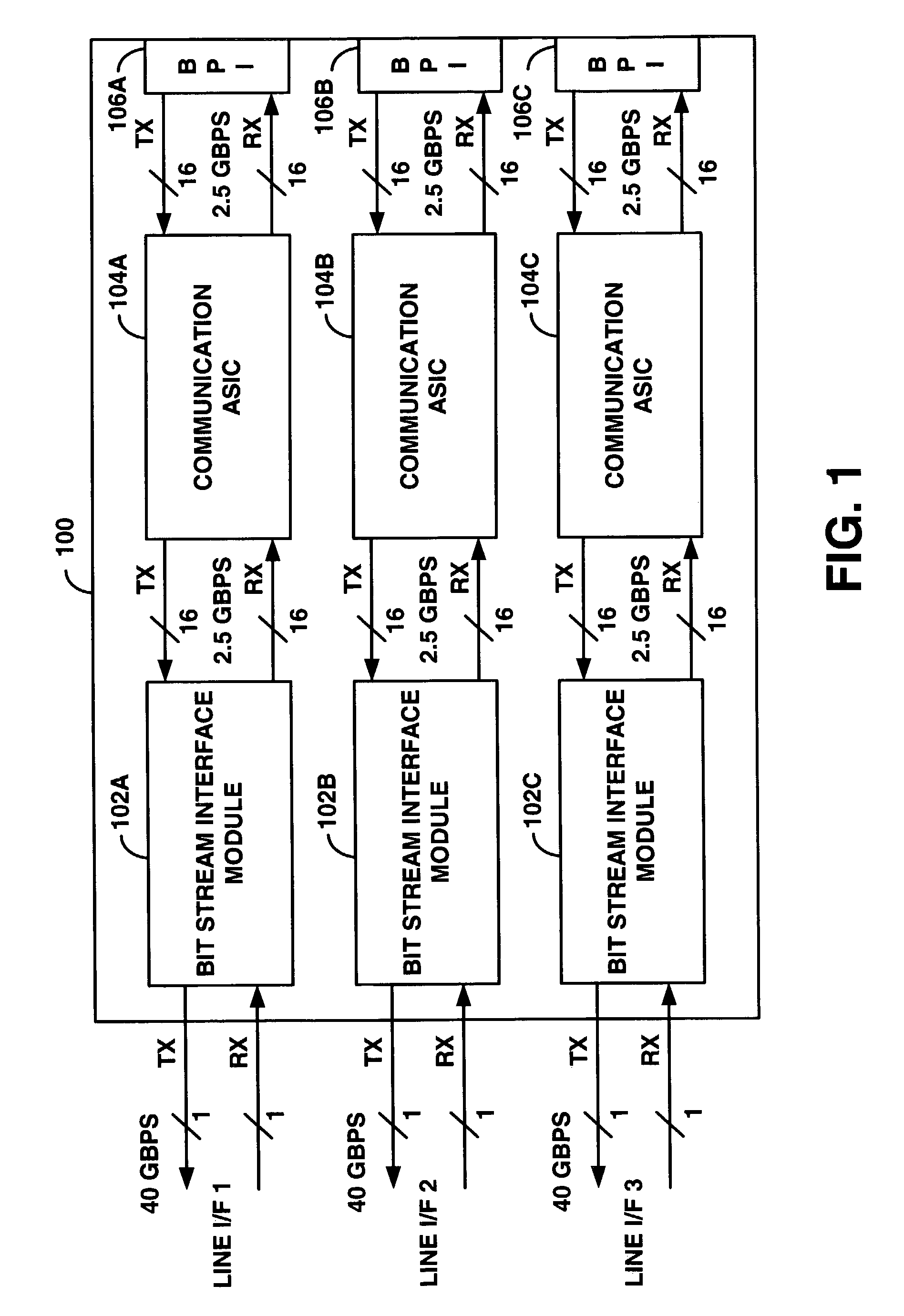
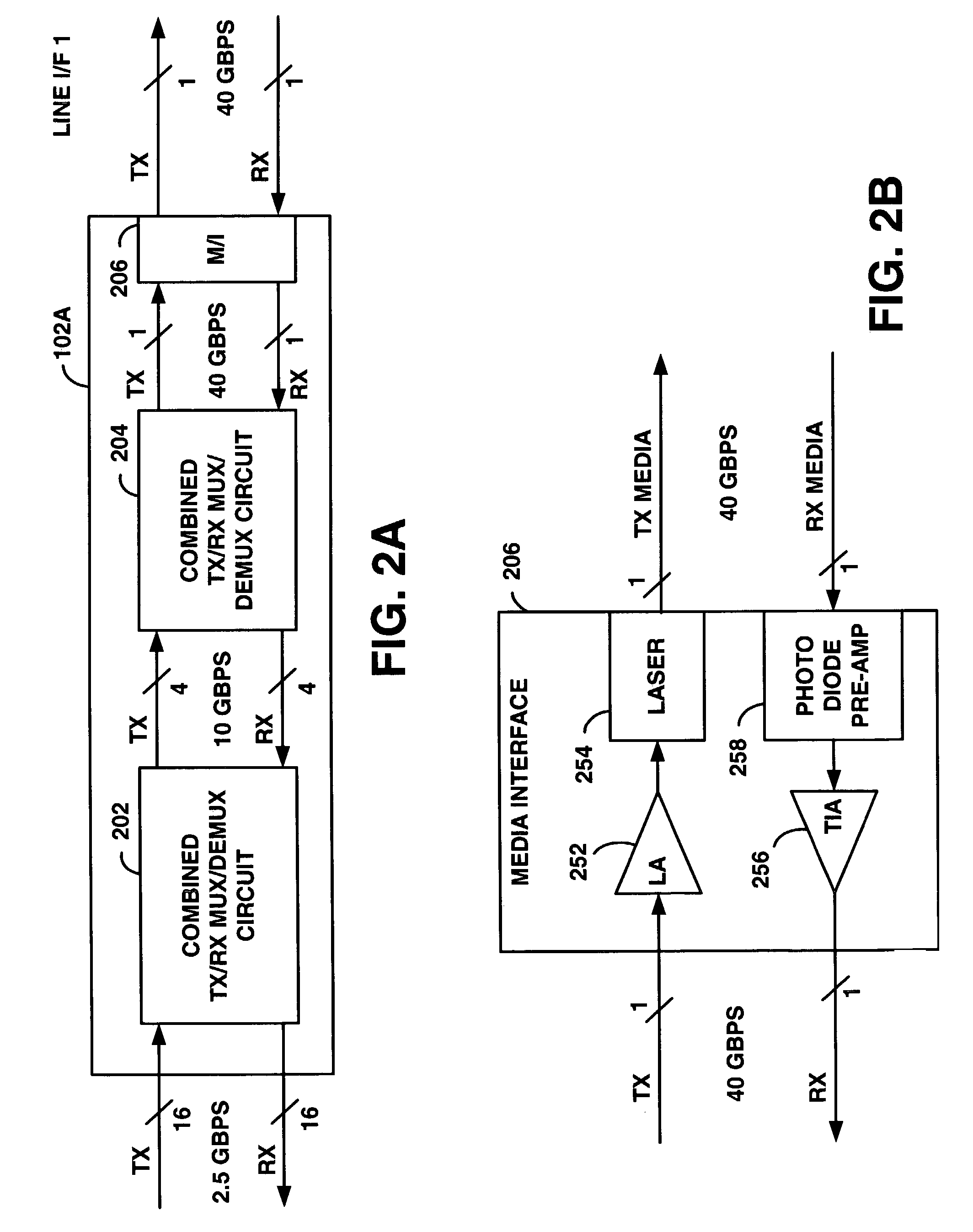
[0044]FIG. 1 provides a block diagram depicting a Printed Circuit Board (PCB) that has mounted thereon a plurality of Bit Stream Interface Module (BSIMs). As shown in FIG. 1, the PCB 100 includes BSIMs 102A, 102B and 102C. The PCB 100 also includes mounted thereupon communication Application Specific Integrated Circuits (ASIC) 104A, 104B, and 104C. The PCB 100 is mounted within a housing that services switching requirements within a particular location or geographic area. Each of the BSIMs 102A, 102B, and 102C couples to a high-speed media such as an optical fiber or other media as known to those skilled in the art, via a respective media interface and supports the OC-768 or the SEC-768 standard at such media interface. On the second side of the BSIMs 102A through 102C, the SFI-5 interface standard is supported...


PUM


Abstract

A multi-stage bit stream multiplexer that divides multiplexing functions between two or more integrated circuits. The first integrated circuit receives 16 bit streams to produce 4 output bits streams with a nominal data rate of 10 GBPS. A second integrated circuit multiplexes the 4 streams and to a bit stream with a data rate of 40 GBPS. The first IC is made in a standard CMOS process while the second IC is made using processes that support higher switching rates. The first IC produces a source-centered double data rate forward transmit clock from a reference clock selectable from either a crystal oscillator, a voltage controlled oscillator using a loop clock from the receive side of the bit stream multiplexer or a reverse clock generated by the second IC. The reverse clock can be selected as the source of the reference either by default, or in response to a specific condition.

Description

CROSS REFERENCE TO RELATED APPLICATION[0001]This application claims priority to U.S. Provisional Application Ser. No. 60 / 403,457, filed Aug. 12, 2002, which is incorporated herein by reference in its entirety for all purposes.BACKGROUND OF THE INVENTION[0002]1. Technical Field of the Invention[0003]The present invention relates generally to communication systems; and more particularly to high-speed serial bit stream multiplexing.[0004]2. Description Of Related Art[0005]The structure and operation of communication systems is generally well known. Communication systems support the transfer of information from one location to another location. Early examples of communication systems included the telegraph and the public switch telephone network (PSTN). When initially constructed, the PSTN was a circuit switched network that supported only analog voice communications. As the PSTN advanced in its structure and operation, it supported digital communications. The Internet is a more recentl...

Claims


Application Information

Patent Timeline
Patent Type & Authority Patents(United States)
IPC IPC(8): H04J3/02H04J3/04H04J3/06H04L7/00
CPCH04J3/04H04J3/0629H04J3/0685H04L7/0008
Inventor NEJAD, MOHAMMADGHIASI, ALI
Owner AVAGO TECH INT SALES PTE LTD
Why Eureka
Try Eureka