Method for designing semiconductor integrated circuit, semiconductor integrated circuit and program for designing same

a technology of reset signal and integrated circuit, which is applied in the direction of program control, generating/distributing signals, instruments, etc., can solve the problems of more severe timing constraints on reset signals, inability to adopt tree structures, and inability to meet time constraints (clock cycles or the like) sometimes to design reset signals, etc., to achieve the effect of facilitating the design of reset signals, reducing product cost, and reducing development period

Inactive Publication Date: 2008-10-28
SOCIONEXT INC
View PDF5 Cites 4 Cited by
  • Summary
  • Abstract
  • Description
  • Claims
  • Application Information

AI Technical Summary

Benefits of technology

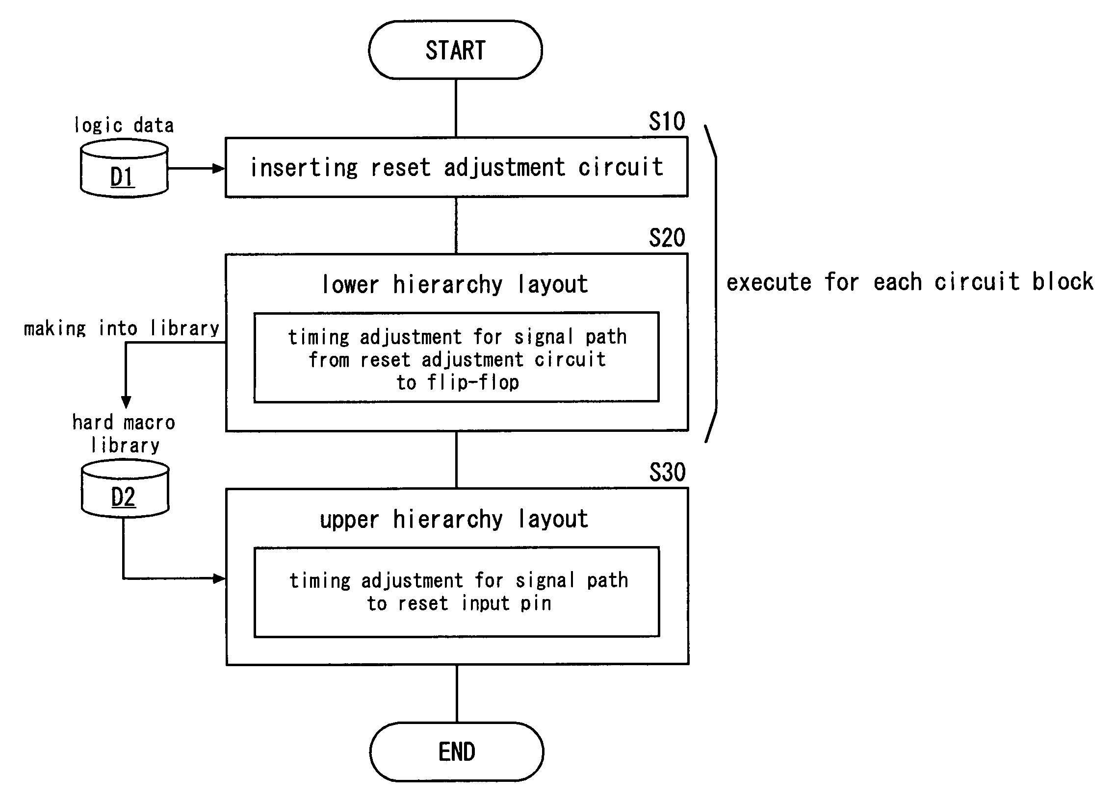
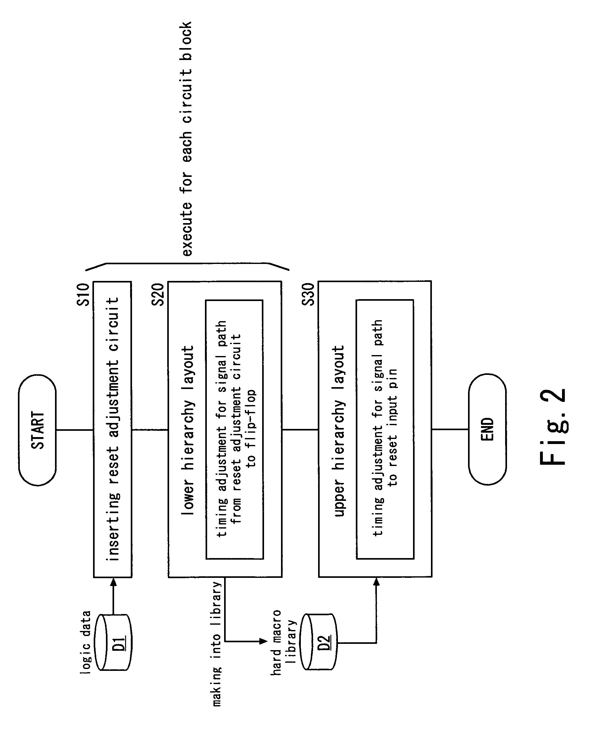
[0014]It is an object of the present invention to make the setup time and the hold time of a reset signal that are prescribed for each reset input pin small and constant irrespective of a circuit configuration. It is another object of the present invention to facilitate designing a reset signal in hierarchical design of a semiconductor integrated circuit. It is still another object of the present invention to shorten the development period of a semiconductor integrated circuit and to curtail product cost.
[0020]The setup time and the hold time of the reset signal that are prescribed respectively for the reset input pins of the circuit blocks can be made small and constant, so that timing constraint on the reset signal in the upper hierarchy design can be relaxed. Consequently, in the upper hierarchy design, even when the cycle of the clock signal is small, the timing adjustment for the paths of the reset signal can be implemented easily. In other words, designing the reset signal can be facilitated. Therefore, the development period of the semiconductor integrated circuit can be shortened and product cost can be curtailed.

Problems solved by technology

Therefore, if hierarchical design is implemented by combining a large number of lower hierarchy blocks, timing constraint (clock cycle or the like) cannot be sometimes satisfied (state of difficulty in timing closure) in upper hierarchy design since the setup time and the hold time are prescribed at different values respectively for the signal input pins of the plural lower hierarchy blocks receiving a common signal.
Therefore, the smaller the clock cycle is, the more severe timing constraint on the reset signal is.
This method is effective in a case where the reset signals are collectively designed in the entire LSI, but in a case of the hierarchical design, the tree structure cannot be adopted to portions included in the lower hierarchy blocks since the paths of the reset signal include inner parts of the lower hierarchy blocks whose physical design has been completed.
For this reason, a timing adjustment effect by the adoption of the tree structure is limited.
Consequently, it requires a large number of man-hours to design the reset signal.
This results in a longer design period of the LSI and increased product cost.
This method is effective for a general signal synchronizing with a clock signal, but is not effective for a signal such as a reset signal that is not synchronized with the clock signal and is supplied from a reset input pin directly to a reset pin of each flip-flop.

Method used


Image

  • Method for designing semiconductor integrated circuit, semiconductor integrated circuit and program for designing same
  • Method for designing semiconductor integrated circuit, semiconductor integrated circuit and program for designing same
  • Method for designing semiconductor integrated circuit, semiconductor integrated circuit and program for designing same

Examples


Embodiment Construction

[0032]In a preferable example of the first or the second aspect of the present invention, a first synchronization circuit of the reset adjustment circuit outputs as a first internal signal the reset signal from the reset input pin, in synchronization with the clock signal. A logic operation circuit of the reset adjustment circuit activates an internal reset signal to be supplied to the flip-flips, in synchronization with the activation transition of the reset signal. The logic operation circuit deactivates the internal reset signal in synchronization with deactivation transition of the first internal signal. Therefore, the activation timing of the internal reset signal is the same as that of the reset signal, and is irrespective of the clock signal. On the other hand, the deactivation timing of the internal reset signal is the same as that of the first internal signal and is synchronous with the clock signal. Therefore, if the timing adjustment using the clock signal as a reference ...


PUM


Abstract

In lower hierarchy design in which a plurality of circuit blocks are independently designed, a reset adjustment circuit propagating deactivation transition of a reset signal to flip-flops in synchronization with a clock signal is inserted immediately after a reset input pin in each circuit block, and timing adjustment using the clock signal as a reference is implemented for signal paths of the reset signal from the reset adjustment circuit to the flip-flops. In upper hierarchy design in which an entire semiconductor integrated circuit is designed, timing adjustment using the clock signal as a reference is implemented for signal paths of the reset signal, according to setup times and hold times of the reset signal that are prescribed respectively for the reset input pins of the circuit blocks.

Description

CROSS REFERENCE TO RELATED APPLICATION[0001]This application is based upon and claims the benefit of priority from Japanese Patent Application No. 2004-341676, filed on Nov. 26, 2004, the entire contents of which are incorporated herein by reference.BACKGROUND OF THE INVENTION[0002]1. Field of the Invention[0003]The present invention relates to a semiconductor integrated circuit, and more particularly, to a technique of designing a reset signal in the semiconductor integrated circuit.[0004]2. Description of the Related Art[0005]In designing a large-scale LSI, as a method to effectively utilize intellectual property and reduce a design period, known is hierarchical design (hierarchical layout design) in which physical design (layout design) of each lower hierarchy block is independently implemented, and physical design of the entire LSI (upper hierarchy) is implemented, using the lower hierarchy blocks (including hard macro which is a library of layout data) whose physical design has...

Claims


Application Information

Patent Timeline
Patent Type & Authority Patents(United States)
IPC IPC(8): G06F17/50G06F1/04G06F1/12
CPCG06F1/24G06F17/505G06F17/5068G06F30/39G06F30/327
Inventor KOSUGI, NAOTODAIJO, JIRO
Owner SOCIONEXT INC
Why Eureka
Try Eureka