
Method for manufacturing a plate-shaped workpiece

a technology of workpieces and plates, applied in the direction of solid-state diffusion coating, plasma technique, electric/magnetic/electromagnetic heating, etc., can solve the problem of significant inhomogeneity in treatment for some applications

Active Publication Date: 2008-11-11
EVATEC
View PDF9 Cites 4 Cited by
  • Summary
  • Abstract
  • Description
  • Claims
  • Application Information

AI Technical Summary

Benefits of technology

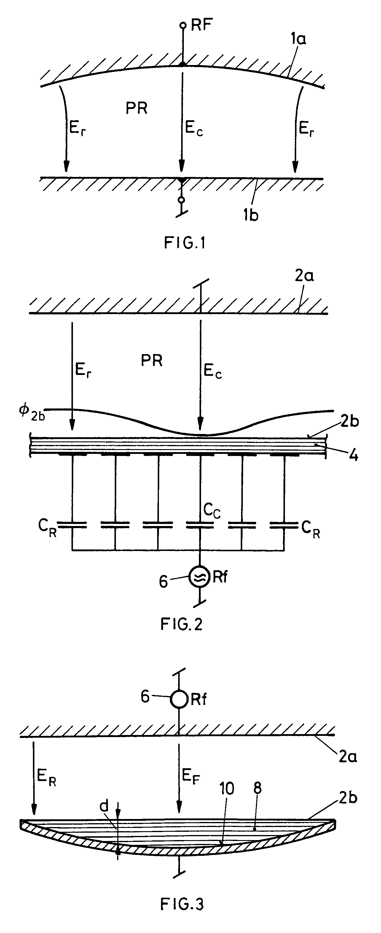
[0039]It should be emphasized again that—if a chamber is formed—it is essential to prevent that in this chamber formed between metallic coupling face and backside of the dielectric plate configuration parasitic plasma discharges occur, which would eliminate the effect of this chamber as an areally distributed coupling capacitance. As is known to the person skilled in the art, this is ensured by dimensioning the spacing ratio between metallic coupling face and backside of the dielectric plate configuration, in any case less than the dark space distance valid in the particular process.

Problems solved by technology

Such significant inhomogeneities in the treatment are not acceptable for some applications, such as in particular in the production of said liquid crystals, TFT or plasma displays, as well as in photovoltaics, and here especially in the production of solar cells.

Method used


Image

  • Method for manufacturing a plate-shaped workpiece
  • Method for manufacturing a plate-shaped workpiece
  • Method for manufacturing a plate-shaped workpiece

Examples


Embodiment Construction

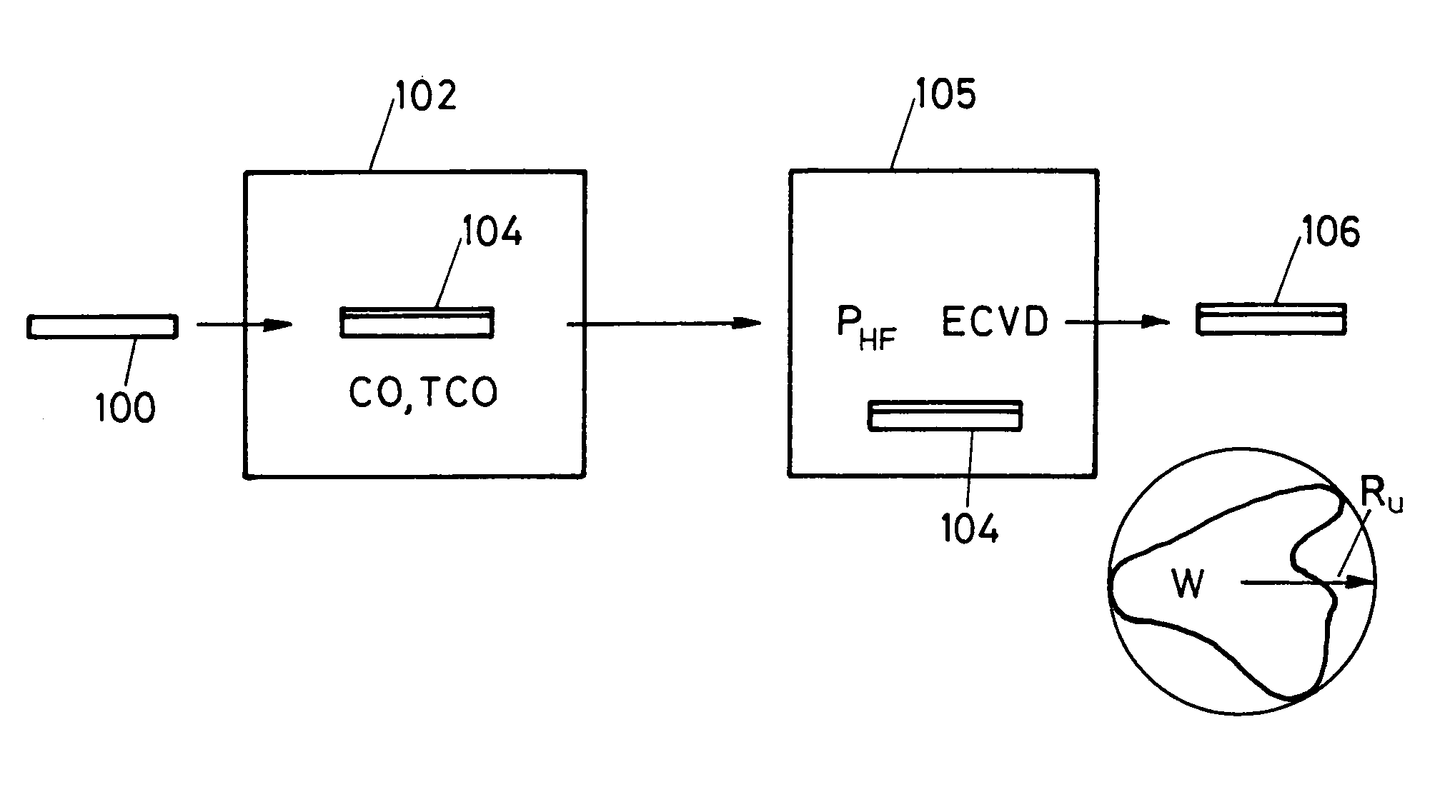
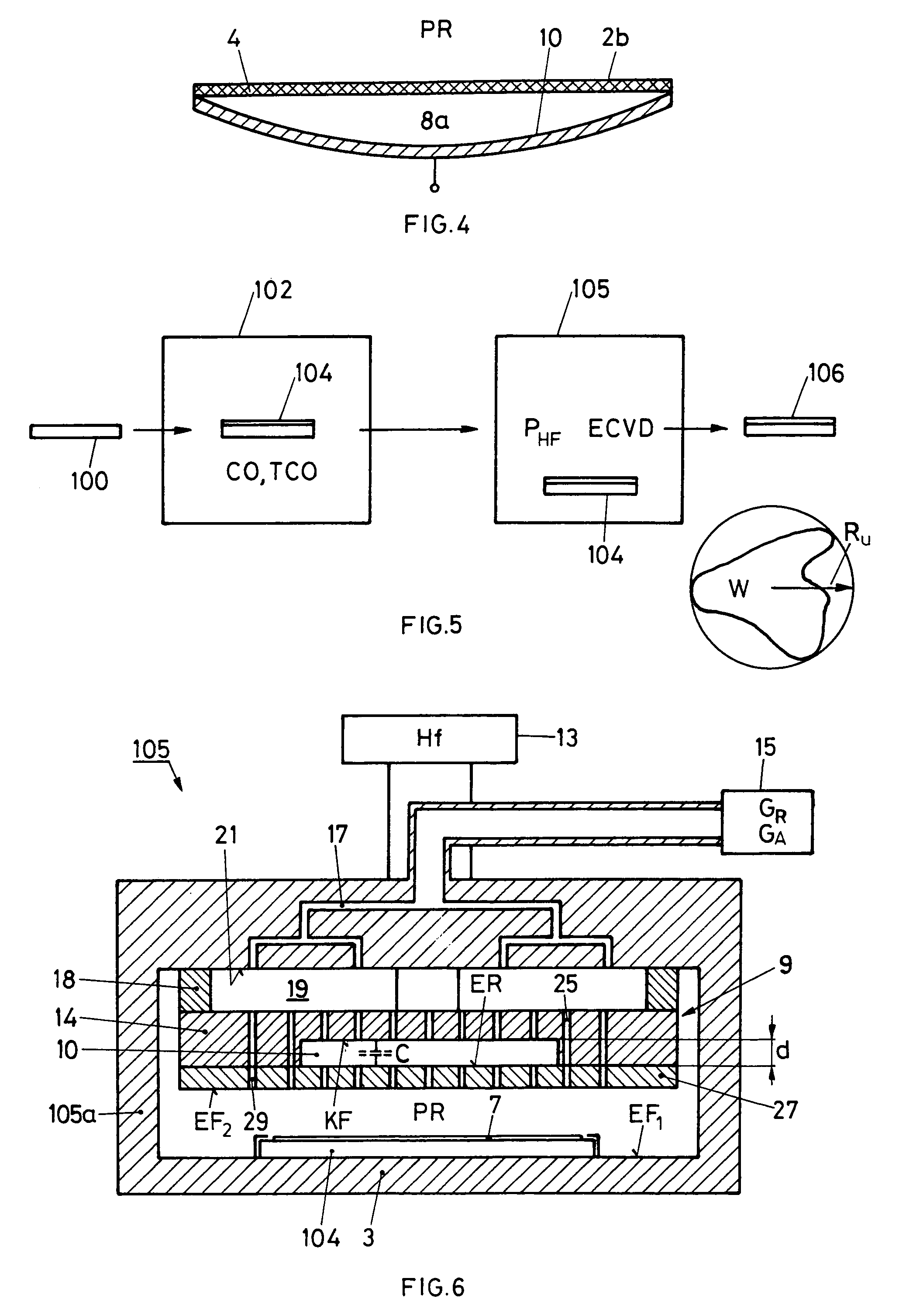
[0074]In conjunction with a simplified block diagram the sequence of the method according to the invention is depicted in FIG. 5. A dielectric substrate 100 is at least partially coated in a first vacuum coating station 102, for example a station for reactive magnetron sputtering, with a layer whose material has a specific resistance , for which applies

10−5 Ωcm≦≦10−1Ωcm

and specifically such, that the resulting surface resistance RS of the layer is in the following range:

0S≦104 Ω□.

[0075]The lower limit can approximate 0, since the surface resistance RS is a function of the thickness of the deposited layer. This thickness DS of the layer is preferably selected as follows:

10 nm≦DS≦5 μm

especially if the deposited layer material, as is far preferred, is an electrically conducting oxide (CO), optionally a transparent electrically conducting (TCO). For this purpose at least one of the following materials InO2, ZnO or SnO2 is deposited on the dielectric substrate 100 in doped or undoped for...


PUM

PropertyMeasurementUnit
Diameteraaaaaaaaaa
Electrical resistanceaaaaaaaaaa
Electrical resistivityaaaaaaaaaa

Abstract

A method for producing a disk shaped workpiece with a dielectric substrate includes treatment in a plasma process volume between two electrode faces bounding a high-frequency plasma discharge. One electrode face is of dielectric material and is at a high-frequency potential with a varying distribution along the face. The other electrode face is metallic. Reactive gas is introduced into the process volume through an aperture pattern. The dielectric substrate, before treatment, is at least regionally coated with a layer material to whose specific resistance applies: 10−5 Ωcm≦≦10−1 Ωcm, and to the resulting surface resistance RS of the layer applies: 0<RS≦104 Ω. Subsequently, the coated substrate is positioned on the metallic electrode face and is etched or coated reactively under plasma enhancement in the plasma process volume.

Description

FIELD AND BACKGROUND OF THE INVENTION[0001]The present invention builds on a method for the production of a disk-form or disk-shaped workpiece based on a dielectric substrate, which production method comprises the treatment in a plasma process volume, formed between two opposing electrode faces in a vacuum receptacle.DEFINITION[0002]We are defining “electrode face” as a surface freely exposed to the plasma process volume.[0003]In said method, on which the present invention builds, an electric high-frequency field is generated between the electrode faces and therewith in the process volume charged with a reactive gas, a high-frequency plasma discharge is generated. The one electrode face is herein comprised of a dielectric material and a high-frequency potential is applied to it with a specified distribution varying along the face. The distribution of the electric field in the plasma process volume is set through the potential distribution on the dielectric electrode face. In the met...

Claims


Application Information

Patent Timeline
IPC IPC(8): H05H1/03C23C16/00C23C16/509H01J37/32H05H1/24
CPCC23C16/45565C23C16/5096H01J37/32541
Inventor BUECHEL, ARTHURWIELAND, WERNERELLERT, CHRISTOPHSANSONNENS, LAURENT
Owner EVATEC
Learn More