High efficiency optical diffraction device

a high-efficiency, optical diffraction technology, applied in the field of diffractive optical elements, can solve the problems of inability to achieve high-efficiency optical diffraction, inability to meet the requirements of high-efficiency optical diffraction, and limited multi-level manufacturing process costs, and achieve the effect of high efficiency

Active Publication Date: 2008-11-18
PARRIAUX OLIVIER M
View PDF6 Cites 142 Cited by
  • Summary
  • Abstract
  • Description
  • Claims
  • Application Information

AI Technical Summary

Benefits of technology

[0020]The device of the invention allows high and possibly close to 100% diffraction efficiency in a non-coplanar diffraction configuration as the excitation of a leaky mode propagating in a direction contained in the incidence plane and having the same polarization as the incident beam suffices to cancel the Fresnel reflection, therefore to give rise to close to 100% diffraction efficiency, essentially regardless of the polarization state of the −1st diffracted order.

Problems solved by technology

One of the hurdles in diffractive optics technologies is the difficulty of obtaining high diffraction efficiency.
This is a costly multilevel manufacturing process which is presently limited to elements of small angular aperture.
This solution is not available yet as a manufacturing technology.
This technology is only suitable for manufacturing large volumes of identical elements and suffers from the thermal instability and ageing of the replicable material.

Method used


Image

  • High efficiency optical diffraction device
  • High efficiency optical diffraction device
  • High efficiency optical diffraction device

Examples


Embodiment Construction

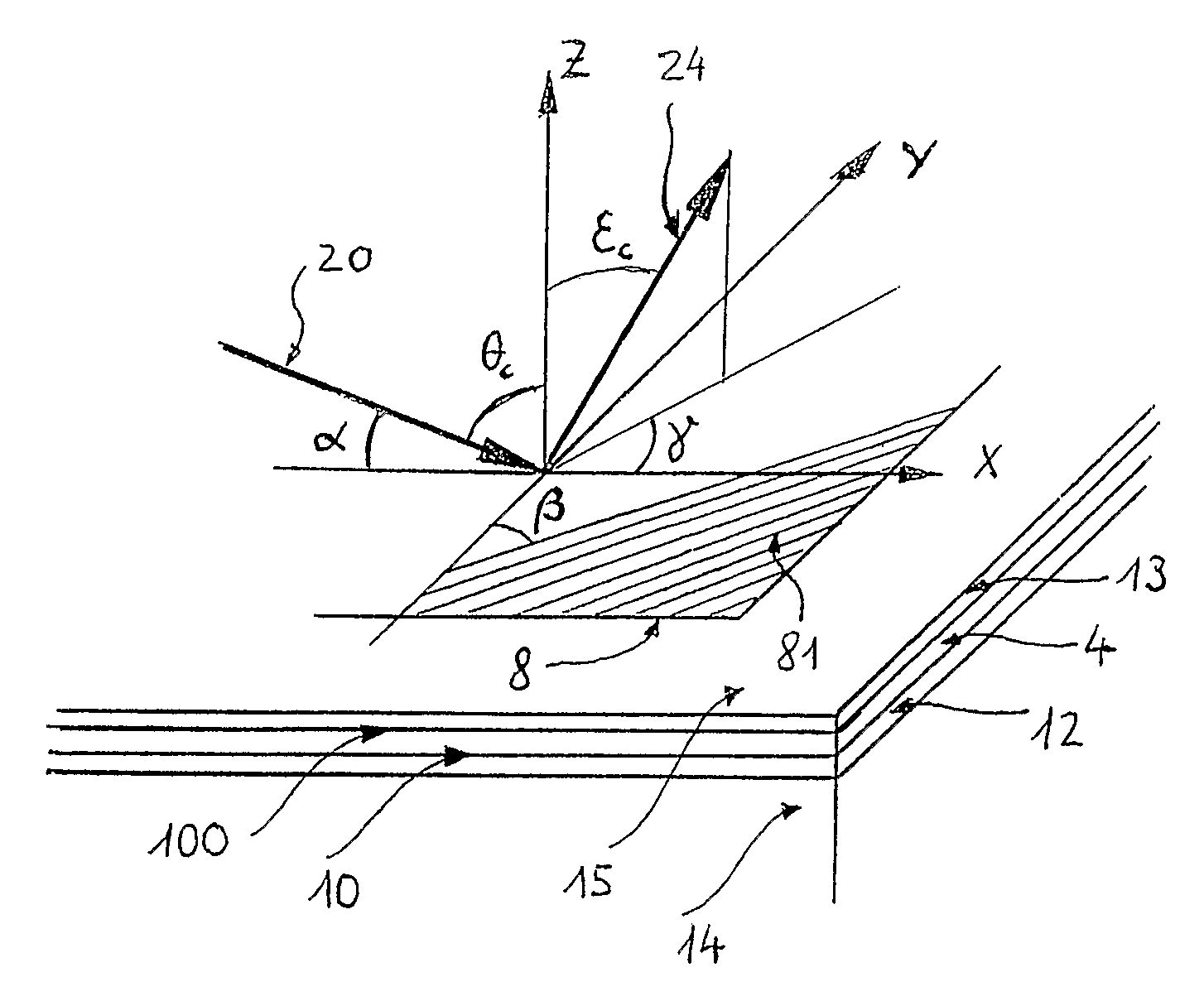
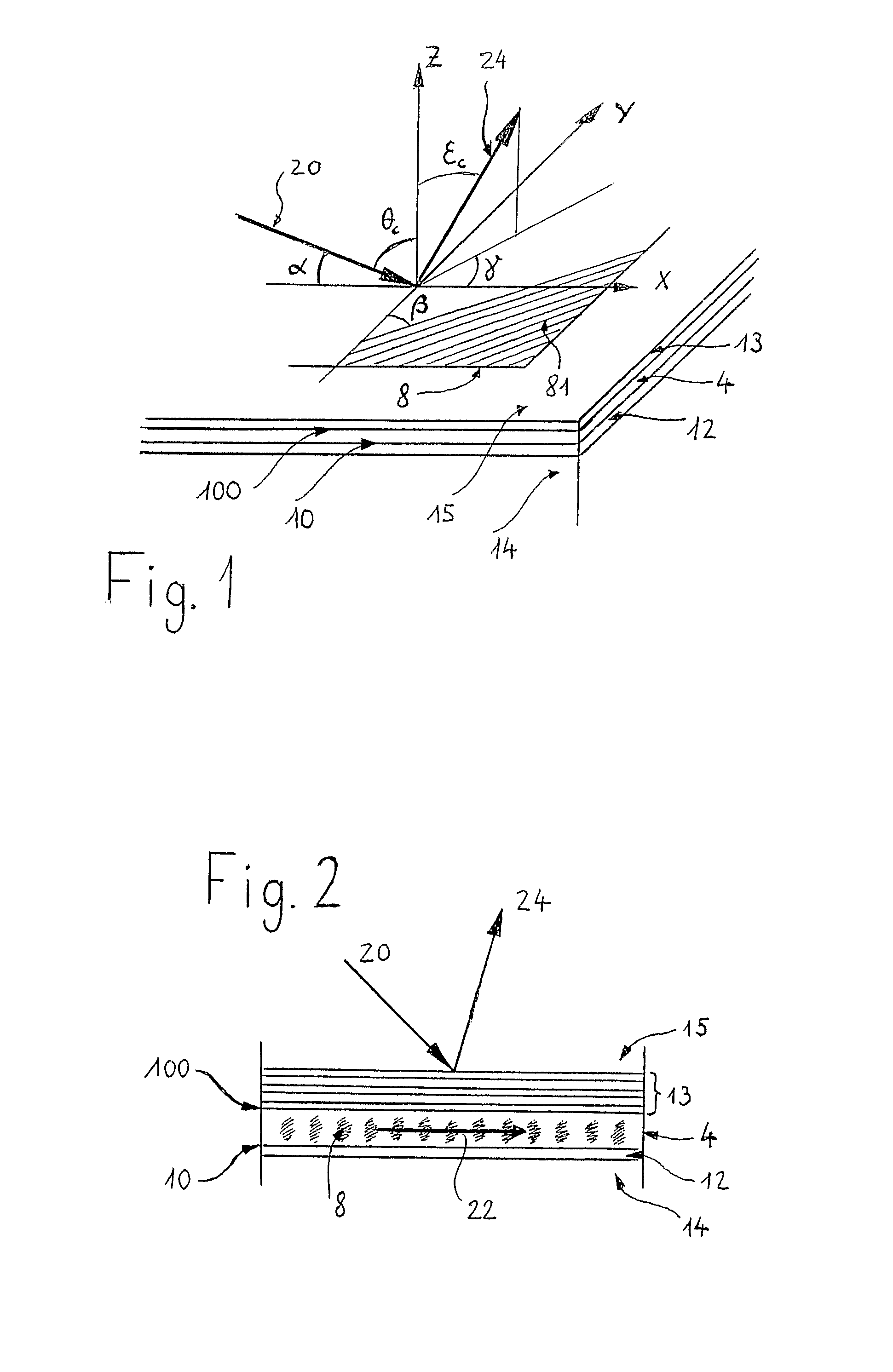
[0059]FIG. 1 is the perspective view of a device according to the invention in the direct (x, y, z) space. The dielectric or semiconductor layer 4 of refractive index nf and mean height H is bounded by the highly reflective structure 12 at its lower side 10 and by the semi-reflective structure 13 at its upper side 100. The refractive index nf of layer 4 may be a continuous graded index or a stepwise function of coordinate z. By highly reflective structure 12 we understand an interface which has substantially a 100% reflection between two media. This interface can be a simple metal surface, or a dielectric or semiconductor multilayer mirror, or a dielectric dioptre under total internal reflection condition, or a resonantly reflective grating, or a set of two phase shifted gratings. By semi-reflective structure 13 we understand a reflective layer or film (dielectric or semiconductor or metallic) or a multilayer structure or a resonantly reflective grating or similar structure. Under t...


PUM


Abstract

Lightwave diffraction device formed of a dielectric layer (4), a mirror (12) arranged at the lower face (10) of said layer, a semi-reflective structure (13) arranged at the upper face (100) of said layer, and a diffractive structure (8) arranged in said layer or on its faces. The height (H) of the layer is chosen so as to substantially satisfy the resonance condition for at least one leaky mode propagating in said layer for at least one given incident wave having a determined wavelengthλ and a determined incidence angle θc. Next, the diffractive structure is arranged so that there is no propagating positive diffracted order, and so that all negative orders other than the −1st propagating order have zero or a relatively small diffraction efficiency, the reflected −1st order propagating in a direction non-parallel to the incident wave. This diffraction device allows a high diffraction efficiency of up to 100% for the −1st order.

Description

[0001]This is a National Phase Application in the United States of International Patent Application No. PCT / EP2005 / 004357 filed Apr. 22, 2005, which claims priority on European Patent Application No. 04009672.9, filed Apr. 23, 2004, and International Patent Application No. PCT / EP2004 / 008583, filed Jul. 30, 2004. The entire disclosures of the above patent applications are hereby incorporated by reference.FIELD OF THE INVENTION[0002]The present invention concerns Diffractive Optical Elements and in particular an optical diffraction device of large diffraction efficiency for the sole −1st propagating diffraction order and particularly easy to manufacture, such device having a layer in which light can propagate in a leaky mode, this layer being associated with a diffraction structure and being bounded at a lower side by a highly reflective structure.BACKGROUND OF THE INVENTION[0003]Diffractive Optical Elements (DOEs) are now widely used in technical optics because they are planar elemen...

Claims


Application Information

Patent Timeline
Patent Type & Authority Patents(United States)
IPC IPC(8): G02B6/34G02B27/44F21V8/00G02B5/18G02B5/28G02B5/32G02B6/12G02B6/124
CPCG02B5/1814G02B5/1828G02B5/1861G02B5/289G02B5/32G02B6/0016G02B6/124G02B6/34G02B2006/12164G03H1/0408G03H2250/42
Inventor PARRIAUX, OLIVIER M.
Owner PARRIAUX OLIVIER M
Why Eureka
Try Eureka