Reprogrammable metal-to-metal antifuse employing carbon-containing antifuse material

a metal-to-metal and anti-fuse technology, applied in the direction of semiconductor devices, semiconductor/solid-state device details, instruments, etc., can solve the problems of low reliability during programming, dielectric materials that require complex manufacturing techniques, and sub-substrat-level anti-fuses

Inactive Publication Date: 2008-12-02
MICROSEMI SOC
View PDF56 Cites 216 Cited by
  • Summary
  • Abstract
  • Description
  • Claims
  • Application Information

AI Technical Summary

Problems solved by technology

However, because of high development costs and high manufacturing tooling costs of such circuits, it is advantageous for integrated circuits to be configured or programmed by the user to implement a desired application.
A programming process disrupts the antifuse material and forms a filament between the two electrodes.
There are known problems with substrate-level antifuses.
Some of the suggested dielectric materials require complex manufacturing techniques and have low reliability during programming.
Some programmed antifuses may have a finite resistance on the order of several hundred to several thousand ohms which may render them relatively unsuitable for use in high speed circuits, and also result in high power consumption when a large number of circuits are switching simultaneously.
This can place a limit on device operating speed because antifuses on a single line act as capacitors linked in parallel, such that the sum of the individual capacitances of the unprogrammed antifuses can slow data signals undesirably.
Finally, substrate antifuses consume a lot of chip area.
Antifuse capacitance, as described above, is also a problem for metal-to-metal antifuses.
Amorphous silicon antifuses alleviate this problem by providing a relatively thick antifuse layer, however, amorphous silicon antifuses exhibit relatively high leakage currents.
If this layer is too thin, it will not be an effective barrier, and if it is too thick, it will appreciably raise the programming voltage of the antifuse.
One factor that contributes to read disturb is the presence of any significant quantity of aluminum in the antifuse conductive links due to electromigration of the aluminum.
However, reducing the thickness of the antifuse material layer results in an increase in the capacitance of the antifuse in its unprogrammed state.
This increased capacitance has a negative impact on the product speed.
One problem in employing amorphous carbon as the antifuse material layer has been that it can fail to adhere to a metal electrode.
In an amorphous-carbon based antifuse device, the problem of finding a glue layer material is difficult because a suitable glue layer material must adhere to both the metal electrode and the amorphous-carbon antifuse material layer.

Method used


Image

  • Reprogrammable metal-to-metal antifuse employing carbon-containing antifuse material
  • Reprogrammable metal-to-metal antifuse employing carbon-containing antifuse material
  • Reprogrammable metal-to-metal antifuse employing carbon-containing antifuse material

Examples


Embodiment Construction

[0026]Those of ordinary skill in the art will realize that the following description of the present invention is illustrative only and not in any way limiting. Other embodiments of the invention will readily suggest themselves to such skilled persons.

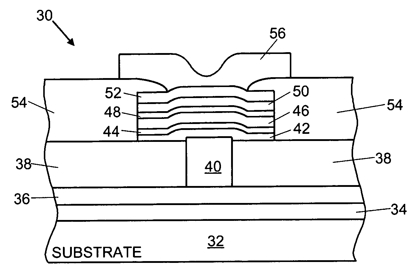
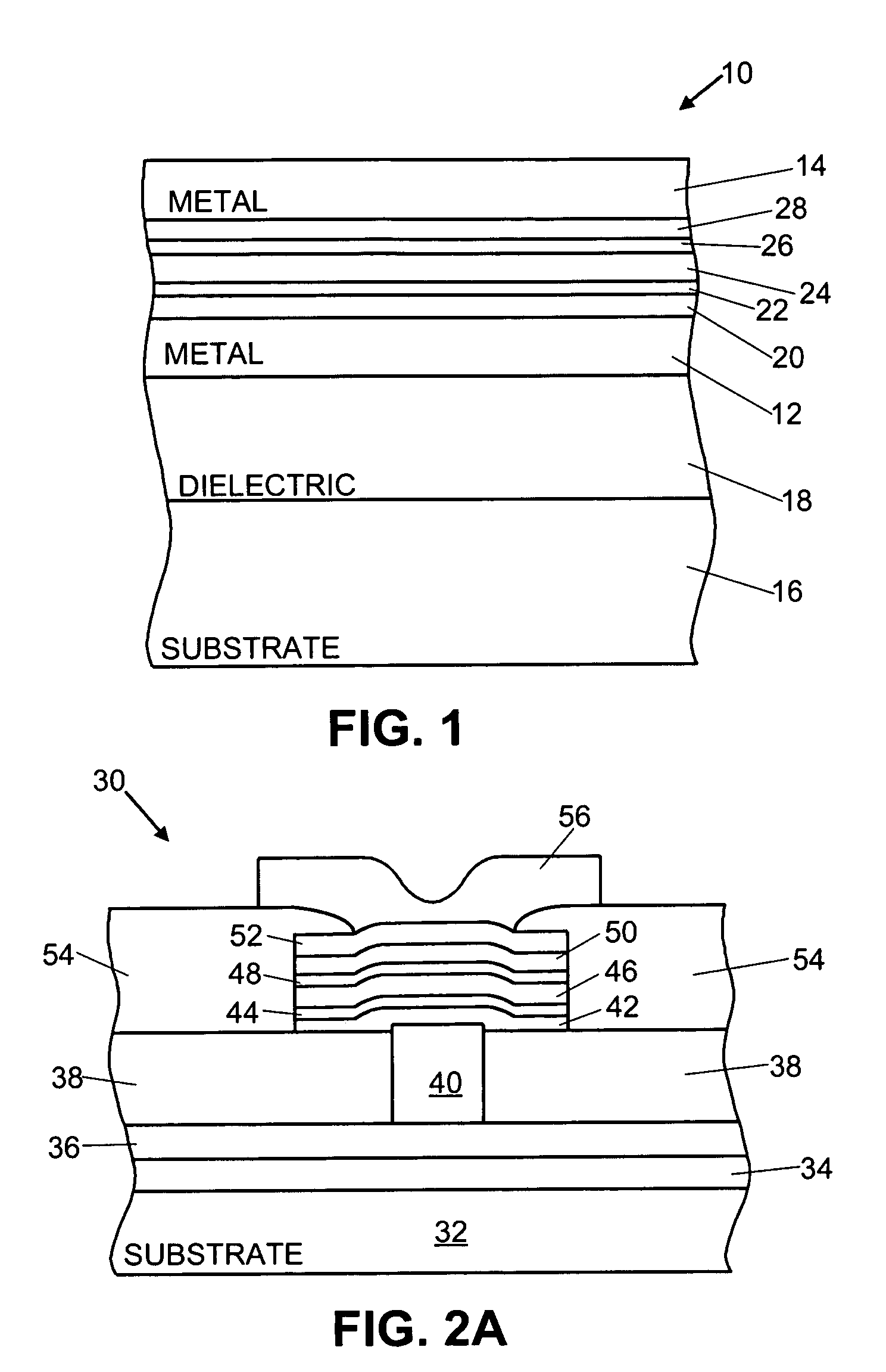
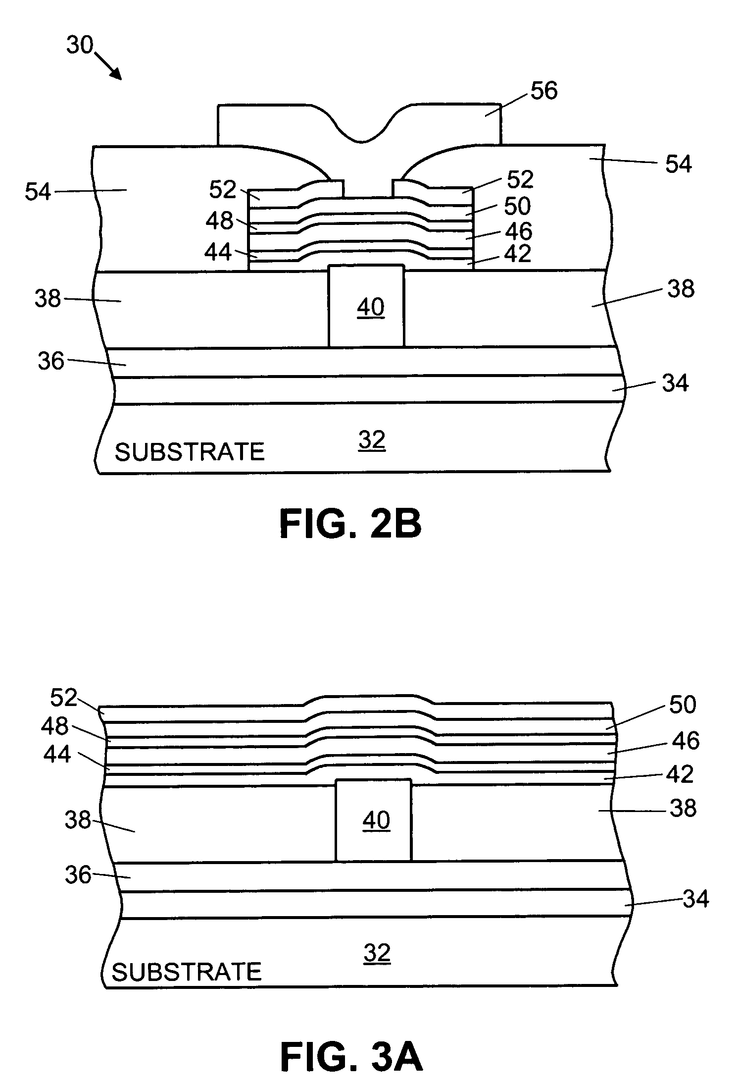
[0027]In FIG. 1, a reprogrammable antifuse 10 according to the present invention is depicted generally in a cross-sectional view. The reprogrammable antifuse 10 is disposed between a lower metal interconnect layer 12 and an upper metal interconnect layer 14. Lower metal interconnect layer 12 and upper metal interconnect layer 14 are disposed above a semiconductor substrate 16 and an intervening insulating layer 18. The antifuse 10 has a lower Ti barrier layer 20, a lower adhesion-promoting layer 22 comprised of a material selected from the group comprising SixCy and SixNy, an antifuse material layer 24 formed from amorphous carbon or amorphous carbon doped with at least one of hydrogen and fluorine, an upper adhesion-promoting layer 26 ...


PUM

PropertyMeasurementUnit
thicknessaaaaaaaaaa
thicknessaaaaaaaaaa
thicknessaaaaaaaaaa

Abstract

A reprogrammable metal-to-metal antifuse is disposed between two metal interconnect layers in an integrated circuit. A lower barrier layer is formed from Ti. A lower adhesion-promoting layer is disposed over the lower Ti barrier layer. An antifuse material layer selected from a group comprising at least one of amorphous carbon and amorphous carbon doped with at least one of hydrogen and fluorine is disposed over the lower adhesion-promoting layer. An upper adhesion-promoting layer is disposed over the antifuse material layer. An upper Ti barrier layer is disposed over the upper adhesion-promoting layer.

Description

RELATED APPLICATIONS[0001]This application is a continuation-in-part of co-pending application Ser. No. 09 / 972,825, filed Oct. 2, 2001 and Ser. No. 10 / 331,144, filed Dec. 27, 2002, now U.S. Pat. No. 6,965,156 assigned to the same assignee as the present invention.BACKGROUND[0002]1. Field of the Invention[0003]The present invention relates to amorphous carbon metal-to-metal antifuse structures. More particularly, the present invention relates to reprogrammable amorphous carbon metal-to-metal antifuse structures employing adhesion layers and titanium (Ti) barrier layers.[0004]2. The Background Art[0005]Integrated electronic circuits are typically fabricated with all internal connections set during the manufacturing process. However, because of high development costs and high manufacturing tooling costs of such circuits, it is advantageous for integrated circuits to be configured or programmed by the user to implement a desired application. Such circuits are called programmable circuit...

Claims


Application Information

Patent Timeline
Patent Type & Authority Patents(United States)
IPC IPC(8): H01L29/00H01L31/0312
CPCH01L23/5252G11C17/16H01L2924/3011H01L2924/0002H01L2924/00
Inventor ISSAQ, A. FARIDHAWLEY, FRANKMCCOLLUM, JOHN
Owner MICROSEMI SOC
Why Eureka
Try Eureka