

Method enabling a standard CMOS fab to produce an IC to sense three-dimensional information using augmented rules creating mask patterns not otherwise expressible with existing fab rules
a technology of augmented rules and image sensors, applied in the direction of material analysis using wave/particle radiation, nuclear engineering, and video system scanning details, can solve the problems of difficult to approximate the focal distance to an object or subject, luminosity-based systems that do not work well, and time-consuming processes, etc., to achieve effective color resolution of cameras or sensors according, improve detection signal characteristics, and reduce overhead
- Summary
- Abstract
- Description
- Claims
- Application Information
AI Technical Summary
Benefits of technology
Problems solved by technology
Method used
Image

Examples
Embodiment Construction
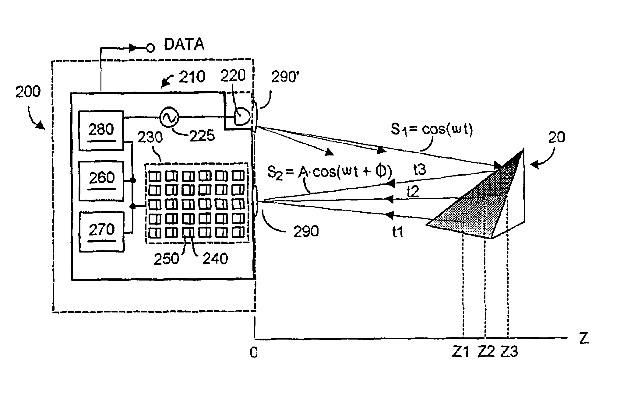
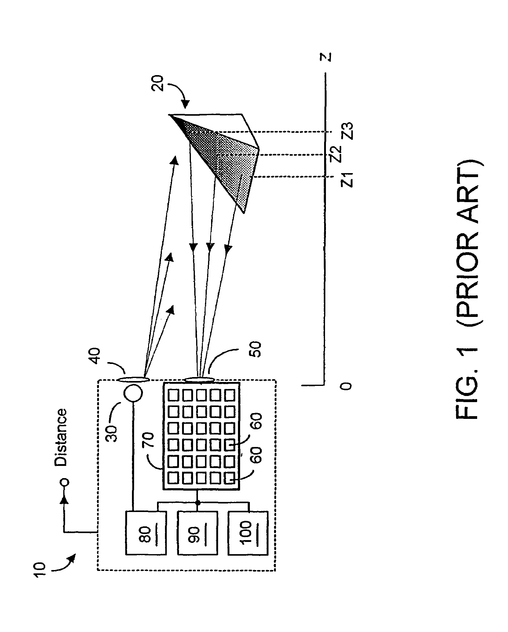
[0091]Before describing the inventions set forth in the three referenced provisional patent applications, it may be useful to first describe the invention(s) of U.S. Pat. No. 6,580,496, hereafter “the '496 invention” or U.S. Pat. No. 6,515,740. As the '496 and '740 patents had the same specification, reference to the inventions of either will be denoted herein as being to the '496 invention.
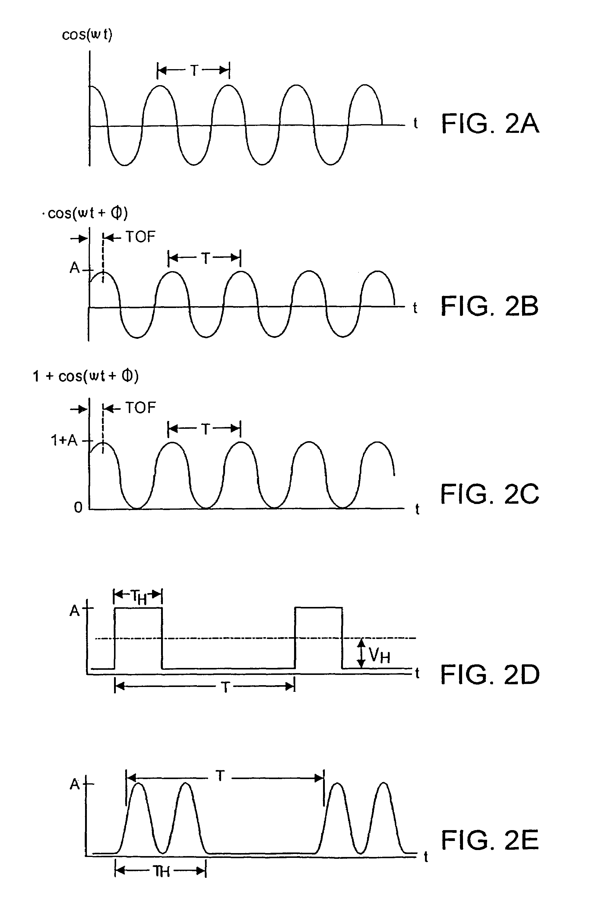
[0092]That invention advantageously transmitted and detected optical energy that was periodic with a high frequency component, and relied upon phase shift between transmitted and detected waveforms to discern time-of-flight (TOF) and thus z-distance data. Although pulsed-type periodic waveforms could be used, the '496 invention will be described with respect to the emission and detection of sinusoidal waveforms, as such waveforms are rather easily analyzed mathematically. However it is to be understood that periodic pulsed waveforms with a high frequency component including imperfect sinusoidal w...
PUM
| Property | Measurement | Unit |
|---|---|---|
| peak power | aaaaa | aaaaa |
| peak power | aaaaa | aaaaa |
| pulse width | aaaaa | aaaaa |
Abstract
Description
Claims
Application Information