Capacitance multiplier circuit

a technology of capacitance multiplier and capacitor, applied in the direction of pulse automatic control, pulse manipulation, pulse technique, etc., can solve the problems of inability to implement relatively high-quality capacitors, capacitor parasitics may be relatively large, and the series resistance of a conventional transistor-based current mirror implementation of a capacitance multiplier may be inacceptably larg

Inactive Publication Date: 2008-12-16
INTEL CORP
View PDF10 Cites 17 Cited by
  • Summary
  • Abstract
  • Description
  • Claims
  • Application Information

AI Technical Summary

Problems solved by technology

In these cases, it may be difficult to implement relatively high quality capacitors, which fall in the microfarad range, in a physical size that is practical.
One problem with many conventional implementations of capacitance multiplier circuits is that the capacitor parasitics may be relatively large.
In particular, the series resistance of a conventional transistor-based current mirror implementation of a capacitance multiplier may be unacceptably large, particularly in many applications that require a capacitor with a relatively large capacitance.
Another problem that may occur in conventional implementations of capacitance multiplier circuits is that the noise injected into the circuit by the capacitance multiplier may degrade the performance of the associated circuits.
In these cases, the noise of the capacitance multiplier may be large enough to degrade the PLL phase noise performance.
In filter applications, the noise injected by a capacitance multiplier also can be of concern since the injected noise effectively raises the noise floor of the signal.
If the filter is used in a receiver or some other noise critical system, the added noise may not be acceptable.

Method used


Image

  • Capacitance multiplier circuit
  • Capacitance multiplier circuit
  • Capacitance multiplier circuit

Examples


Embodiment Construction

[0015]In the following description, like reference numerals indicate like components to enhance the understanding of the capacitance multiplier circuits through the description of the drawings. Also, although specific features, configurations and arrangements are discussed hereinbelow, it should be understood that such specificity is for illustrative purposes only. A person skilled in the relevant art will recognize that other steps, configurations and arrangements are useful without departing from the spirit and scope of the invention.

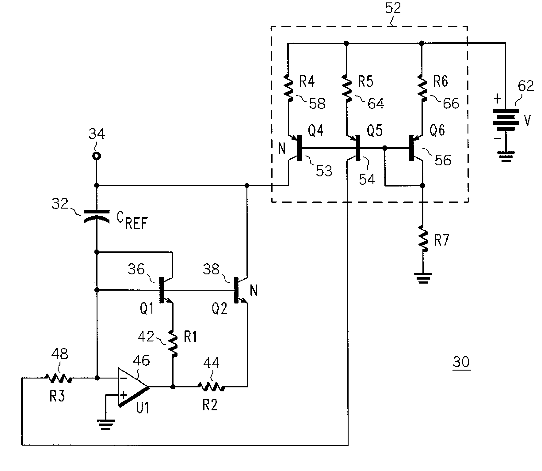
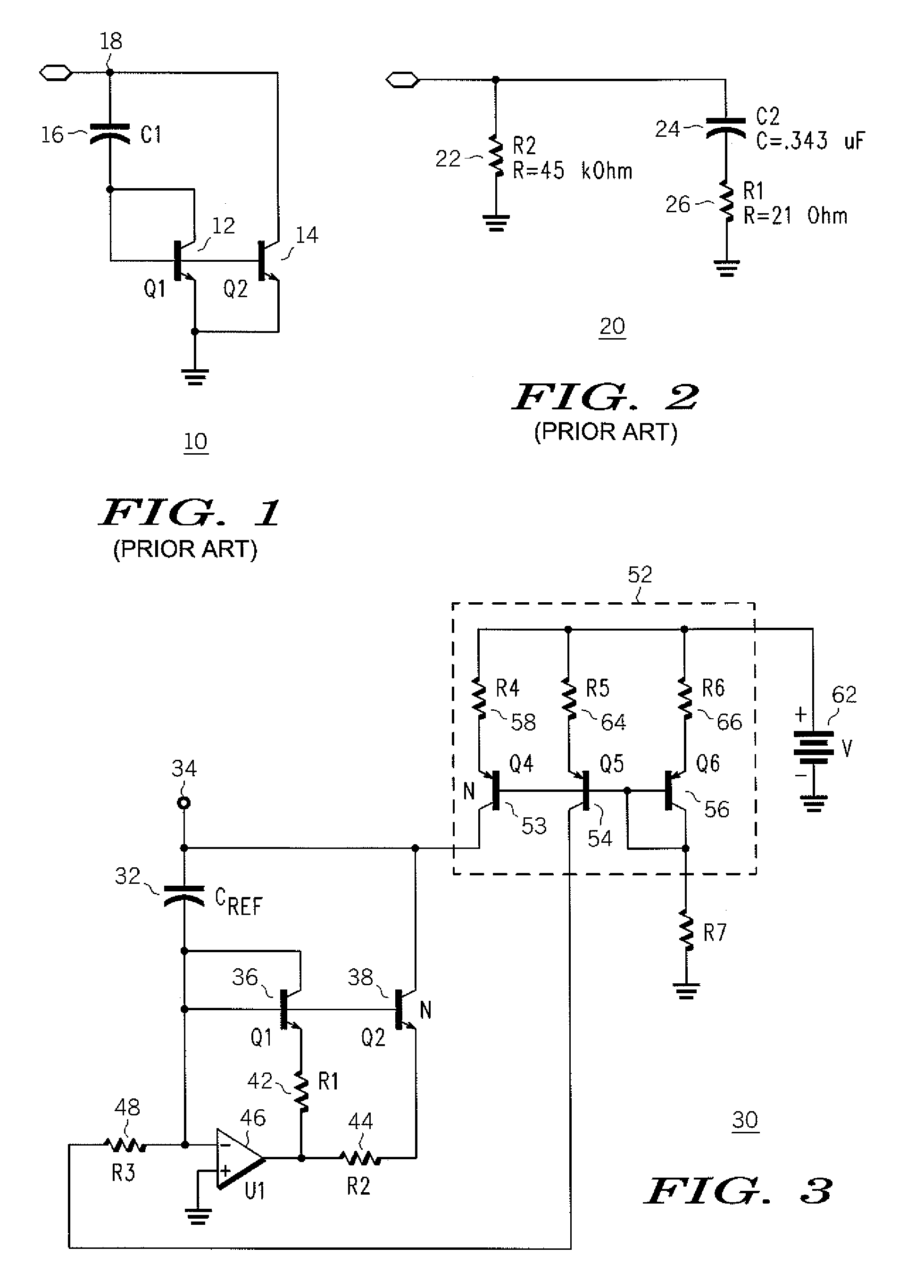
[0016]The capacitance multiplier circuits described herein involve operational amplifier (op-amp)-based capacitance multiplier circuits that reduce the amount of noise injected in the overall application circuit and reduce the parasitic resistance relative to many conventional multiplier methods. The inventive capacitance multiplier circuits are based on an op-amp operating in conjunction with two mirror transistors to form a precision current mirror ...


PUM


Abstract

An integrated circuit including a capacitance multiplier having reduced parasitics and injected noise compared to conventional multiplier methods. The integrated circuit includes a reference capacitor and a current mirror arrangement coupled to the reference capacitor. The current mirror arrangement, which includes a current gain factor N, varies the capacitance of the reference capacitor by a factor of N+1, based on the reference capacitor current. The current mirror arrangement includes an operational amplifier operating in conjunction with two mirror transistors to form a current mirror arrangement having little or no series resistance. The current mirror also can include a plurality of resistors configured to reduce the noise from the capacitance multiplier, thus making the capacitance multiplier useful for applications that may require relatively low noise.

Description

BACKGROUND OF THE INVENTION[0001]1. Field of the Invention[0002]The invention relates to capacitance multiplier circuits. More particularly, the invention relates to capacitance multiplier circuits having reduced capacitor parasitics and reduced noise.[0003]2. Description of the Related Art[0004]A capacitance multiplier is an electronic circuit that uses a relatively small physical capacitance to approximate a relatively larger capacitance value. Often, a capacitance multiplier is a transistor configured to multiply the value of a capacitor coupled to the base of the transistor by an amount equal to the transistor's gain, also known as beta (β). In many applications, a capacitance multiplier can be used to reduce the physical size of a capacitor in a design. For example, in an integrated circuit application where the maximum size of an on-chip capacitor may be 10 picofarads (pF) or less, a 20 times (20×) multiplier will allow capacitors of 200 pF or possibly greater to be realized o...

Claims


Application Information

Patent Timeline
Patent Type & Authority Patents(United States)
IPC IPC(8): H03K5/00H03L7/06
CPCH03F1/56H03F3/347H03H11/48H03H11/483H03F2200/456H03F2200/546
Inventor SMITH, JOE M.ENGLISH, GARY P.
Owner INTEL CORP
Why Eureka
Try Eureka