Transmission method and transmitter circuit

a transmitter circuit and transmitter technology, applied in the field of transmission methods and transmitter circuits, can solve the problems of reducing power supply efficiency, wasting excess dc power as heat, and unable to achieve high-efficiency of high-frequency power amplifiers, and achieves excellent high-frequency characteristics, large amplitude, and reduced power consumption and chip area.

Inactive Publication Date: 2008-12-16
PANASONIC CORP
View PDF23 Cites 11 Cited by
  • Summary
  • Abstract
  • Description
  • Claims
  • Application Information

AI Technical Summary

Benefits of technology

[0044]According to this method, the requirements for a gain bandwidth upon amplifying the amplitude component can be relaxed by dividing the band of the amplitude component separated from the broadband modulating signal. Moreover, the sampling frequency for D / A converting the amplitude component can be reduced, resulting in reduction in the power consumption of the D / A conversion. The method can therefore be applied for the broadband signal, which has been difficult to process by the conventional EER method, enabling the transmitter circuit to be highly efficient using the EER method for the broadband modulating signal.
[0068]The second integrated circuit can be fabricated using the high integration process, such as the analog CMOS process or the BiCMOS process, suitable for the analog circuit. The CMOS process or the bipolar process optimized for analog fabrication is superior to the digital CMOS process specialized for microfabrication in terms of the high power characteristics, such as the withstanding voltage, and the resulting circuit can process the analog signal with a large amplitude. The bipolar process has the excellent high-frequency characteristics, allowing the first and second frequency conversion circuits to up-convert or down-convert the modulating signal into the GHz band. Moreover, since it is possible to incorporate the logic circuit, Phase Locked Loop (PLL) can be integrated to integrate the stable signal source.

Problems solved by technology

However, broadbandization of communication has initiated the use of a communication method by a multicarrier such as the Orthogonal Frequency Division Multiplex (OFDM), thereby leading the conventional class A or class AB high-frequency power amplifier not to capable of achieving high-efficiency.
Since the DC power set as such is too large for amplifying the average power, the excess DC power is wasted as heat.
It results in the power supply efficiency being substantially reduced.
Consequently, continuous usable time of, for example, a portable wireless application utilizing a battery as the power supply becomes shorter, causing a practical problem.
As described above, since the OFDM modulated wave has the large PAPR, the linear amplifier operates with the large back off, causing a problem of low efficiency in the high-frequency power amplifier.
Moreover, since the DC component and the fundamental wave component vary intricately against the duty ratio, the class C operation may be less efficient than the class B operation depending on the duty ratio.
As described above, broadbandization of such as the operational amplifier 1907 or the D / A converter, not only increases the power consumption, but also requires a breakthrough of new technology.

Method used


Image

  • Transmission method and transmitter circuit
  • Transmission method and transmitter circuit
  • Transmission method and transmitter circuit

Examples


first embodiment

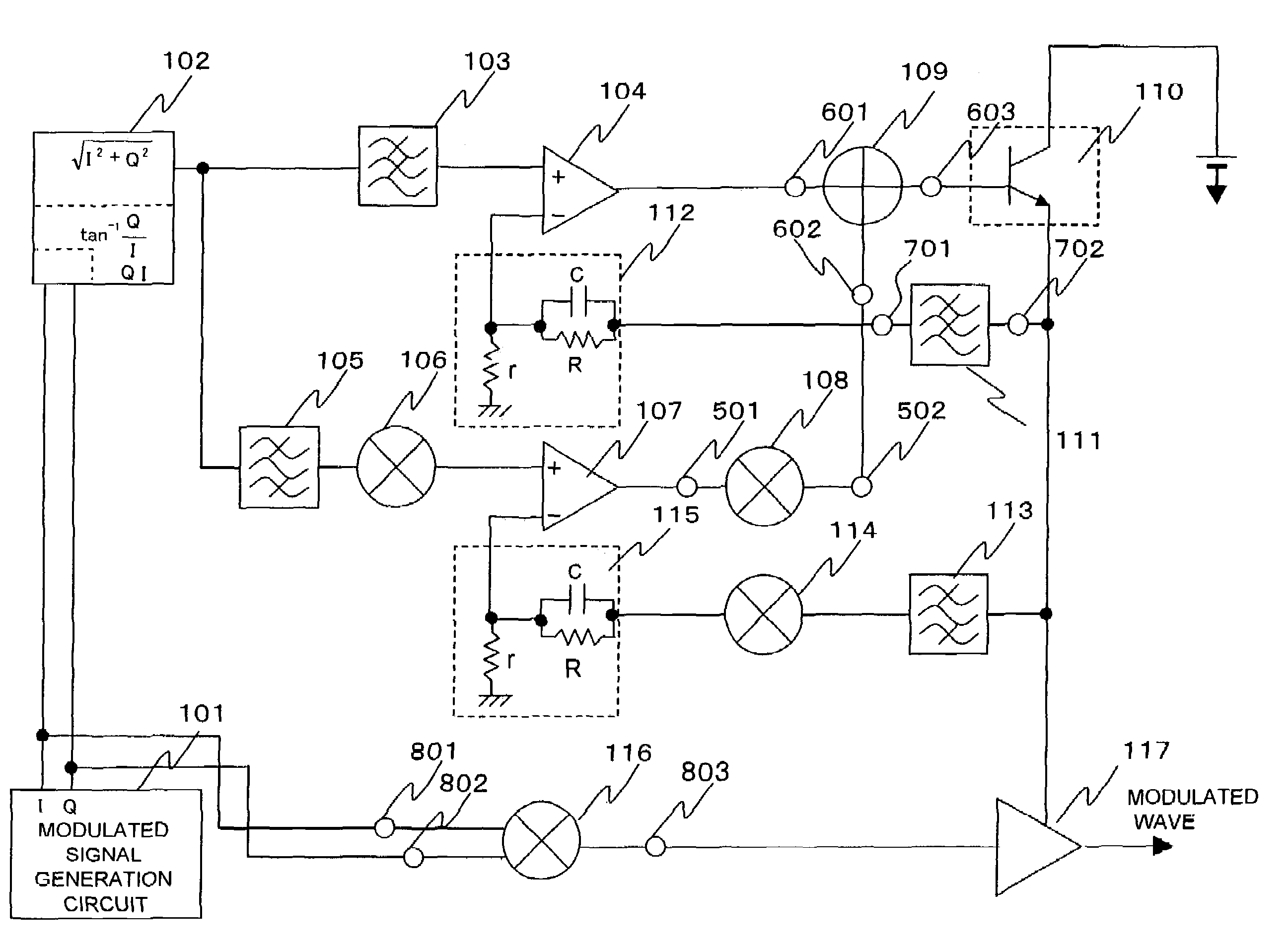
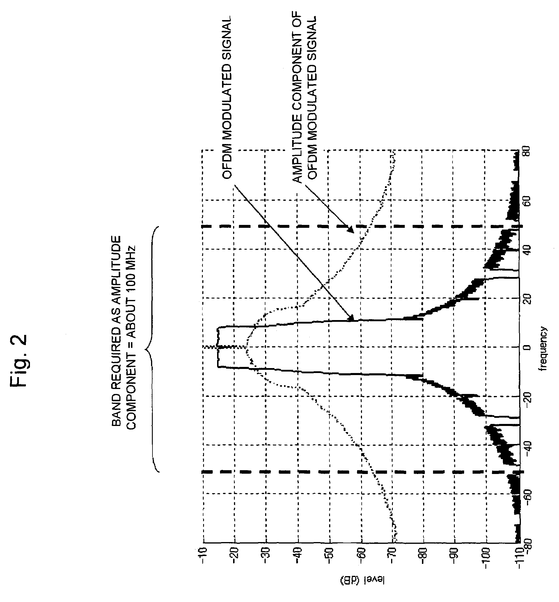
[0090]Hereinafter, the first embodiment according to first and second inventions will be described by reference to the drawings. In this embodiment, an OFDM modulation method is employed as a modulation method. The system using the OFDM modulation method includes, for example, a wireless LAN system of the IEEE 802.11a standard. In the wireless LAN system, a primary modulation such as 64 QAM, 16 QAM, QPSK, or BPSK is performed for each of the orthogonal 52 sub-carriers and then Inverse Fast Fourier Transform (IFFT) is performed, and then all the sub-carriers are added up with each other to obtain the OFDM modulating signal. A symbol rate before the IFFT is set to 20 MHz and the IFFT size is a power value of 2 proximate to 52, i.e., 64. As a result, a data rate provided to the respective sub-carriers after serial parallel conversion is 20 MHz / 64, i.e., 312.5 kHz. Hence, the lowest frequency of the sub-carriers is 312.5 kHz, while the higher-order sub-carrier has the frequency, which i...

second embodiment

[0154]The second embodiment of the present invention will be described by reference to FIG. 10.

[0155]This embodiment is different from the first embodiment that the phase component detected by the detection circuit 102 is input as the modulating signal into the frequency conversion circuit 116.

[0156]Other configurations, as well as their effects and operations, are same as those of the first embodiment, so that the description thereof will be omitted here. The effects obtained by the configuration of this embodiment are as follows. In the first embodiment, when the first frequency conversion means 116 and the high-frequency power amplifier 117 are internally configured by multistage circuits, the back off operation is required for a block or an amplifier stage not involving the saturation operation. The back off operation decreases the efficiency of such block or amplifier stage. However, since the complete constant envelope signal is input in this embodiment, the back off operation...

third embodiment

[0157]The third embodiment of the present invention will be described by reference to FIG. 11.

[0158]FIG. 11 shows a configuration of the third embodiment.

[0159]FIG. 11 shows the configuration which, in the case that the configuration of the first embodiment is implemented using a plurality of integrated circuits, should be included in the respective integrated circuits. The transmitter circuit is configured by three integrated circuits 1101, 1102, and 1103.

[0160]The integrated circuit 1101 integrates the modulating signal generating circuit 101, the detection circuit 102, the frequency selecting circuit 103 and 105, and the frequency conversion circuit 106.

[0161]The integrated circuit 1102 integrates the operational amplifiers 104 and 107, the adder 109, the frequency selecting circuits 111 and 113, the frequency conversion circuits 116, 114 and 108, and the feedback circuits 112 and 115.

[0162]The integrated circuit 1103 integrates the high-frequency power amplifier 117 and the DC c...


PUM


Abstract

An amplitude component of a modulating signal is detected, band-divided by first and second frequency selecting circuits, and an amplitude component of a high-frequency band is down-converted by a first frequency conversion circuit. An amplitude component selected by the first frequency selecting circuit and an amplitude component selected by the first frequency conversion circuit are amplified by first and second operational amplifiers, and a signal amplified by the second operational amplifier is up-converted by a second frequency conversion circuit to be restored to the initial frequency band. Output amplitudes of the first operational amplifier and a second frequency converter are added up by an adder to be direct-current converted. The amplitudes after the direct-current conversion are band-divided by third and fourth frequency selecting circuits, respectively, feedback amounts thereof are adjusted, and then fed back to the first and second operational amplifiers.

Description

BACKGROUND OF THE INVENTION[0001]1. Field of the Invention[0002]The present invention relates to a transmission method and a transmitter circuit for transmitting a high-frequency signal by wireless.[0003]2. Related Art[0004]In a modulating signal involving frequency modulation, in general, especially multi-level modulation such as the quadrature amplitude modulation (QAM), it requires a linear operation for a high-frequency power amplifier disposed in a transmitter circuit for transmitting electricity for an antenna. An operation class A or AB has therefore been utilized for the high-frequency power amplifier.[0005]However, broadbandization of communication has initiated the use of a communication method by a multicarrier such as the Orthogonal Frequency Division Multiplex (OFDM), thereby leading the conventional class A or class AB high-frequency power amplifier not to capable of achieving high-efficiency. In other words, in the OFDM modulation, superposing of sub-carriers generate...

Claims


Application Information

Patent Timeline
Patent Type & Authority Patents(United States)
IPC IPC(8): H04B1/02
CPCH04L27/361H04N5/38H03F1/0205H03F3/24H04L27/2614
Inventor TANABE, MITSURU
Owner PANASONIC CORP
Why Eureka
Try Eureka