Ultraviolet detector

a detector and ultra-violet technology, applied in the field of ultra-violet, can solve the problems of unsatisfactory reliability and lifetime of such configured uv detectors, and the dangerous effects of ultraviolet radiation, so as to improve reliability and uv radiation hardness, and keep good responsivity.

Active Publication Date: 2008-12-30
THE HONG KONG POLYTECHNIC UNIV
View PDF8 Cites 3 Cited by
  • Summary
  • Abstract
  • Description
  • Claims
  • Application Information

AI Technical Summary

Benefits of technology

[0007]An object of the present invention is to develop an UV detector which has significantly improved reliability and UV radiation hardness as compared with the conventional UV detectors, and can keep good responsivity even after a prolonged exposure to a high intensity UV irradiation.
[0008]In order to achieve the above-mentioned object, the present invention provides an UV detector, comprising: a sapphire substrate; a high temperature AlN buffer layer grown on the sapphire substrate; an intermediate temperature GaN buffer layer grown on the high temperature AlN buffer layer; a GaN epitaxial layer deposited on the intermediate temperature GaN buffer layer; a Schottky junction formed on top of the GaN epitaxial layer; and a plurality of ohmic contacts also formed on top of the GaN epitaxial layer, wherein, the high temperature AlN buffer layer and the intermediate temperature GaN buffer layer together form a double buffer layer structure so as to improve the reliability and radiation hardness of the UV detector; and wherein the high temperature AlN buffer layer and the intermediate temperature GaN buffer layer are formed by RF-plasma enhanced MBE growth technology.
[0014]The advantages of the present invention are as follows. With the use of a trilayer structure (the GaN epitaxial layer / the intermediate temperature GaN buffer layer / the high temperature AlN buffer layer), it is possible to greatly improve the reliability and lifetime of the UV detector. This enables the detector to be applied for detecting UV radiation for a long period of time. On the contrary, as to the conventional UV detector without the intermediate temperature buffer layer, the performance will degrades rapidly and the detection result will become inaccurate under a prolonged exposure to UV irradiation.
[0015]According to the present invention, the GaN buffer layer and the AlN buffer layer are formed by radio frequency (hereinafter referred to as “RF”)-plasma enhanced MBE growth. It has been found that both electronic and optic properties of the GaN thin films are improved with the use of this double buffer layer structure. Moreover, experiments have shown that an initial increase in the thickness of the intermediate temperature buffer layer leads to a steady improvement in both the electronic and optic properties of the films. In other words, the electronic and optic properties of the GaN films improve with the increase in the thickness of the intermediate temperature buffer layer. Preferably, the thickness of the intermediate temperature buffer layer is about 800 nm.
[0016]As compared with the UV detector recited in U.S. Pat. No. 5,677,538, the UV detector according to the present invention includes only a Schottky junction, which is formed by depositing a very thin semi-transparent metal film. According to the present invention, the UV detection is performed on the Schottky junction by allowing UV radiation passing through the thin metal film that forms the Schottky junction. Besides, the detector according to the present invention is formed by using a RF-plasma source. Thus, the UV detector according to the present invention is different, both in terms of structure and operation principle, from that disclosed in the U.S. Pat. No. 5,677,538. As a result of this, the UV detector according to the present invention can realize more excellent and stable performance than that disclosed in the above US patent.

Problems solved by technology

However, devastating effects of UV radiation may be very dangerous in some cases.
Moreover, UV radiation may also have devastating effects on eyes, skins, plants and so on.
The reliability and lifetime of such configured UV detector is usually unsatisfactory and the accuracy thereof decreases significantly after a prolonged exposure to high intensity UV irradiation.
A disadvantage of the UV detector with such structure is in that its UV detecting performance will gradually degrade with elapse of time and also a voltage bias is required for the operation of the device.

Method used


Image

  • Ultraviolet detector
  • Ultraviolet detector
  • Ultraviolet detector

Examples


Embodiment Construction

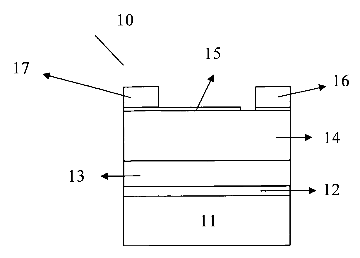
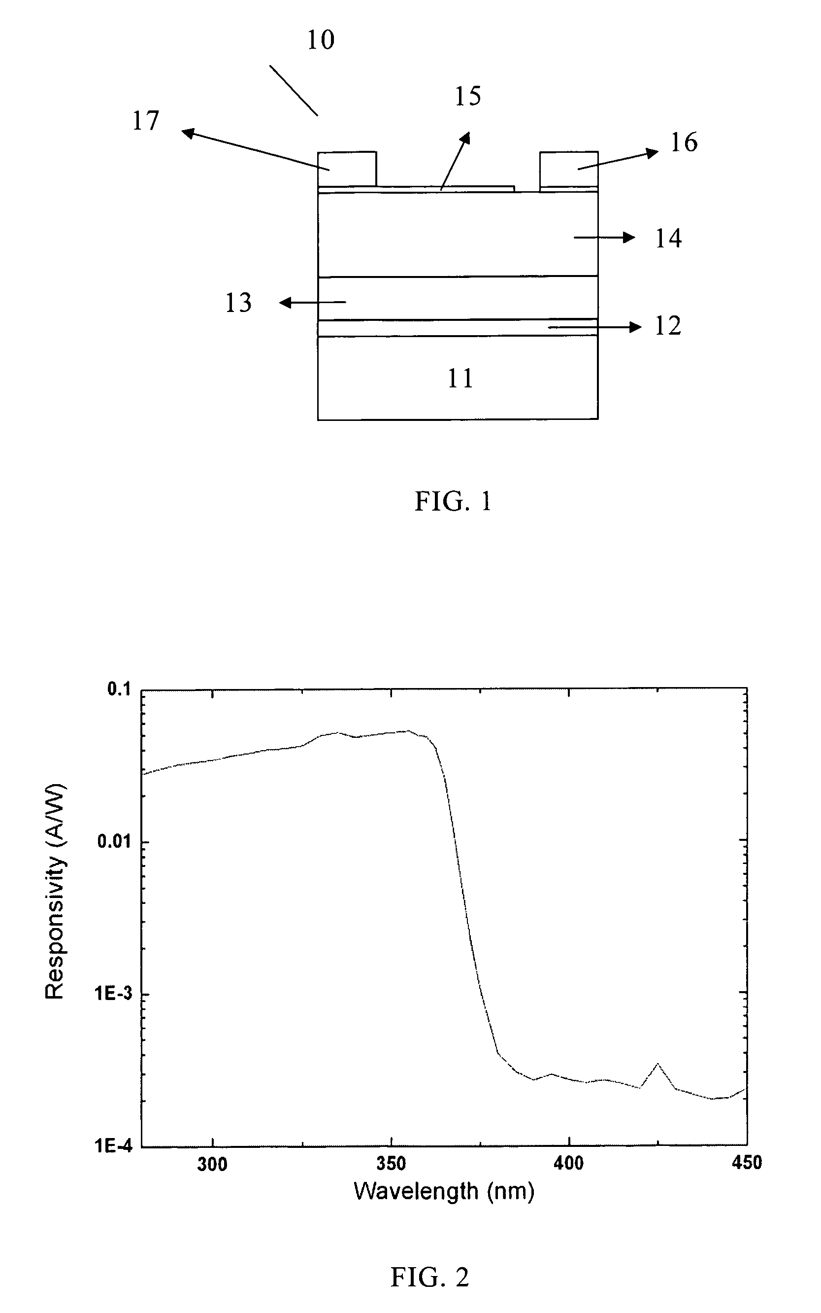
[0023]As shown in FIG. 1, the UV detector 10 of the present invention is configured as follows. Firstly, a high temperature AlN buffer layer 12 is grown on a sapphire substrate 11 at a temperature around 780° C. to have a thickness ranging from 20 nm to 50 nm. Then, on the AlN buffer layer 12, an intermediate temperature GaN buffer layer 13 is grown at a temperature around 600° C. to 680° C. to have a thickness ranging from 400 nm to 800 nm. On the intermediate temperature buffer layer 13, a slightly doped n-type GaN epitaxial layer 14 with doping concentration ranging from 5×1016 cm−3 to about 5×1017 cm−3 is deposited to have a thickness ranging from about 0.5 μm to 1.5 μm. Subsequently, a semi-transparent Schottky junction 15, which consists of a thin layer of nickel (Ni) having a thickness of about 5 nm, is deposited on top of the GaN epitaxial layer 14, and forms the active region of the UV detector. In order to facilitate external contact with the semi-transparent Ni layer, a t...


PUM

PropertyMeasurementUnit
thicknessaaaaaaaaaa
temperatureaaaaaaaaaa
thicknessaaaaaaaaaa

Abstract

An UV detector, comprising: a sapphire substrate; a high temperature AlN buffer layer grown on the sapphire substrate; an intermediate temperature GaN buffer layer grown on the high temperature AlN buffer layer; a GaN epitaxial layer deposited on the intermediate temperature GaN buffer layer; a Schottky junction formed on top of the GaN epitaxial layer; and a plurality of ohmic contacts also formed on top of the GaN epitaxial layer, wherein, the high temperature AlN buffer layer and the intermediate temperature GaN buffer layer together form a double buffer layer structure so as to improve the reliability and radiation hardness of the UV detector; and wherein the high temperature AlN buffer layer and the intermediate temperature GaN buffer layer are formed by RF-plasma enhanced MBE growth technology.

Description

FIELD OF THE INVENTION[0001]The present invention relates to an ultraviolet (hereinafter referred to as “UV”) detector, and more particularly to an UV detector with significantly improved reliability and lifetime by adopting a double buffer layer structure.BACKGROUND ART[0002]UV radiation can be applied to many fields, such as UV sterilization, UV physiotherapy, UV fluorescent analysis and investigation, UV exposure of photolithography and so on. However, devastating effects of UV radiation may be very dangerous in some cases. For example, cultural relics, paintings and calligraphy works, rubber and plastics will undergo an accelerated aging process under a prolonged exposure to UV irradiation. Moreover, UV radiation may also have devastating effects on eyes, skins, plants and so on. It is very important therefore to be able to detect and determine the intensity and amount of UV radiation.[0003]Gallium nitride (hereinafter referred to as “GaN”) material possesses characteristics of ...

Claims


Application Information

Patent Timeline
Patent Type & Authority Patents(United States)
IPC IPC(8): H01L29/732H01L27/095H01L31/00
CPCH01L31/0304H01L31/108H01L31/184Y02E10/544
Inventor SURYA, CHARLESFONG, PATRICK WAI-KEUNG
Owner THE HONG KONG POLYTECHNIC UNIV
Why Eureka
Try Eureka