Imaging tool calibration artifact and method

a technology of calibration artifact and tool, applied in the field of integrated circuit manufacturing, can solve the problems of low information content of artifact structure, poor fov sampling, limited metal accuracy, etc., and achieve the effect of low cos

Active Publication Date: 2009-01-06
IBM CORP +1
View PDF16 Cites 53 Cited by
  • Summary
  • Abstract
  • Description
  • Claims
  • Application Information

AI Technical Summary

Benefits of technology

[0012]It is yet another object of the present invention to provide an artifact and method of using the artifact to achieve the above objects, wherein the artifact provides a calibration target of small size that may be printed in the scribe or kerf areas of s

Problems solved by technology

Metrology accuracy is limited by the within-FOV fidelity of the imaging system.
Conventional imaging system artifact structures gener

Method used


Image

  • Imaging tool calibration artifact and method
  • Imaging tool calibration artifact and method
  • Imaging tool calibration artifact and method

Examples


Embodiment Construction

)

[0042]In describing the preferred embodiment of the present invention, reference will be made herein to FIGS. 1-16 of the drawings in which like numerals refer to like features of the invention.

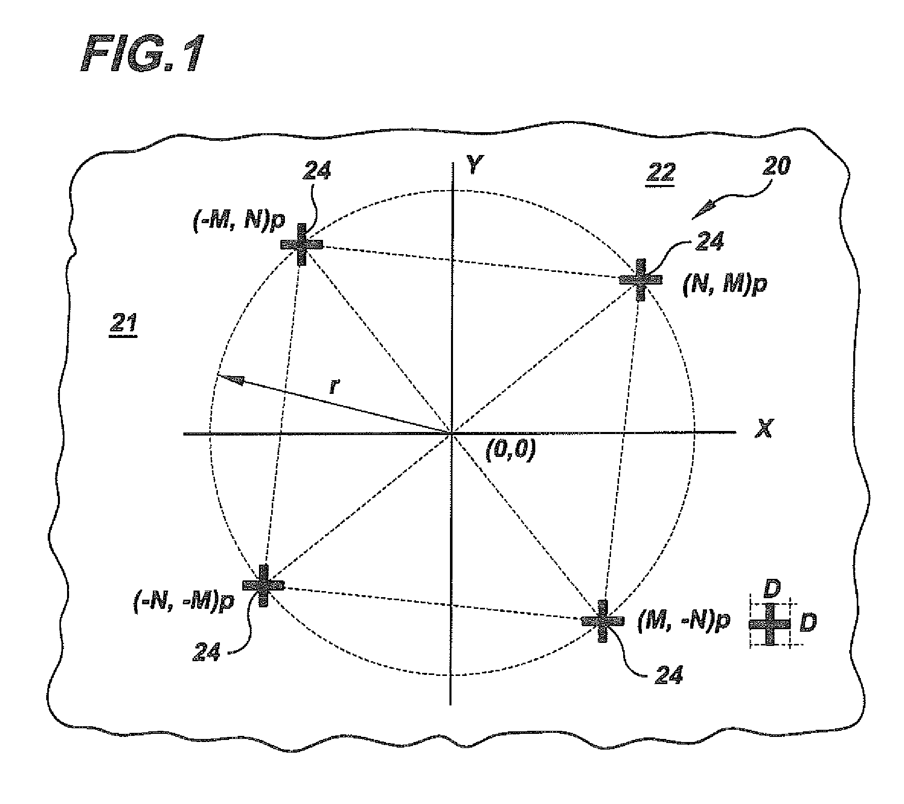
[0043]In deconvolving metrology error sources, one must look at both actual error and tool error. Actual error, (ΔX,ΔY)A, refers to placement errors introduced by pattern fabrication. These errors are dependent on the orientation of the imaging system with respect to the substrate pattern. Systematic and random errors may be introduced by fabrication tools, for example, in stage synchronization, lens aberrations, and the like. These can include printing defects, stitching errors, mark asymmetry, and the like. Systematic and random errors may also be introduced by the non-uniformity of fabrication processes such as coating, baking, developing, etching, and the like. These can include process defects, line-edge roughness, coat / bake / develop / etch non-uniformity, and the like.

[0044]Tool Error (ΔX...


PUM


Abstract

A method of determining and correcting for distortions introduced by an imaging tool. The method includes providing an imaging tool having a field of view (FOV), and creating a target pattern containing a regular array of symmetric sub-patterns having locations spanning the FOV. Using the imaging tool, the method then includes measuring relative position of the sub-pattern images at one or more target orientations, determining tool-induced sub-pattern position deviations from designed locations of the sub-patterns, and applying corrections to compensate for an orientation independent component of the sub-pattern position deviations. The target pattern may be mounted on a stage of the measurement tool, created on a mask used in the lithographic process, or created on a wafer being measured by the measuring tool.

Description

BACKGROUND OF THE INVENTION[0001]1. Field of the Invention[0002]The present invention relates to the manufacture of integrated circuits and, in particular, to a method and system for determining systemic distortions of an overlay error measurement introduced by the imaging system and measurement tool used in lithographic processing of integrated circuits.[0003]2. Description of Related Art[0004]Semiconductor manufacturing requires the sequential patterning of process layers on a single semiconductor wafer. Exposure tools known as steppers or scanners print multiple integrated circuit patterns or fields by lithographic methods on successive layers of the wafer. These exposure tools typically pattern different layers by applying step and repeat lithographic exposure or step and scan lithographic exposure in which the full area of the wafer is patterned by sequential exposure of the stepper fields containing one or more integrated circuits. Typically, 20-50 layers are required to creat...

Claims


Application Information

Patent Timeline
IPC IPC(8): G03F9/00G03C5/00
CPCG03F7/70516G03F7/706G03F7/70633
Inventor AUSSCHNITT, CHISTOPHER P.BINNS, LEWIS A.MORNINGSTAR, JENNIFER L.SMITH, NIGEL
Owner IBM CORP
Why Eureka
Try Eureka