STI stress modification by nitrogen plasma treatment for improving performance in small width devices

a technology of nitrogen plasma treatment and stress modification, which is applied in the field of semiconductor processing, can solve the problems of negative impact on some devices, positive impact on other devices, device improvement, etc., and achieve the effect of increasing the device performance of the p

Inactive Publication Date: 2009-01-20
ALSEPHINA INNOVATIONS INC
View PDF101 Cites 11 Cited by
  • Summary
  • Abstract
  • Description
  • Claims
  • Application Information

AI Technical Summary

Benefits of technology

[0022]A yet further object of the present invention is to provide a method of fabricating isolation regions in which the stress caused by bird beak formation has been modulated to enhance device performance.
[0023]An even further object of the present invention is to provide a method of fabricating isolation regions in which the stress caused by bird peak formation is reduced for NFETs.
[0024]A still further object of the present invention is to provide a method in which stress formation caused by bird beak formation is controlled such that improved device performance, in terms of drive current and on-current, can be achieved for a structure containing both NFETs and PFETs.
[0027]The aforementioned objects and advantages are achieved in the present invention by forming a nitride liner, i.e., a surface nitrided layer, about the trench walls (bottom and sidewalls) by using a plasma nitridation process. Because of the plasma nitridation used in the present invention, the nitride liner penetrates the bottom and sidewalls of the trench so as to form a liner that is present in the interior as well as the exterior of the trench walls. The nitride liner formed using the plasma nitridation process of the present invention serves to prevent the formation of bird beaks in the isolation region during a subsequent CMOS oxidation step.
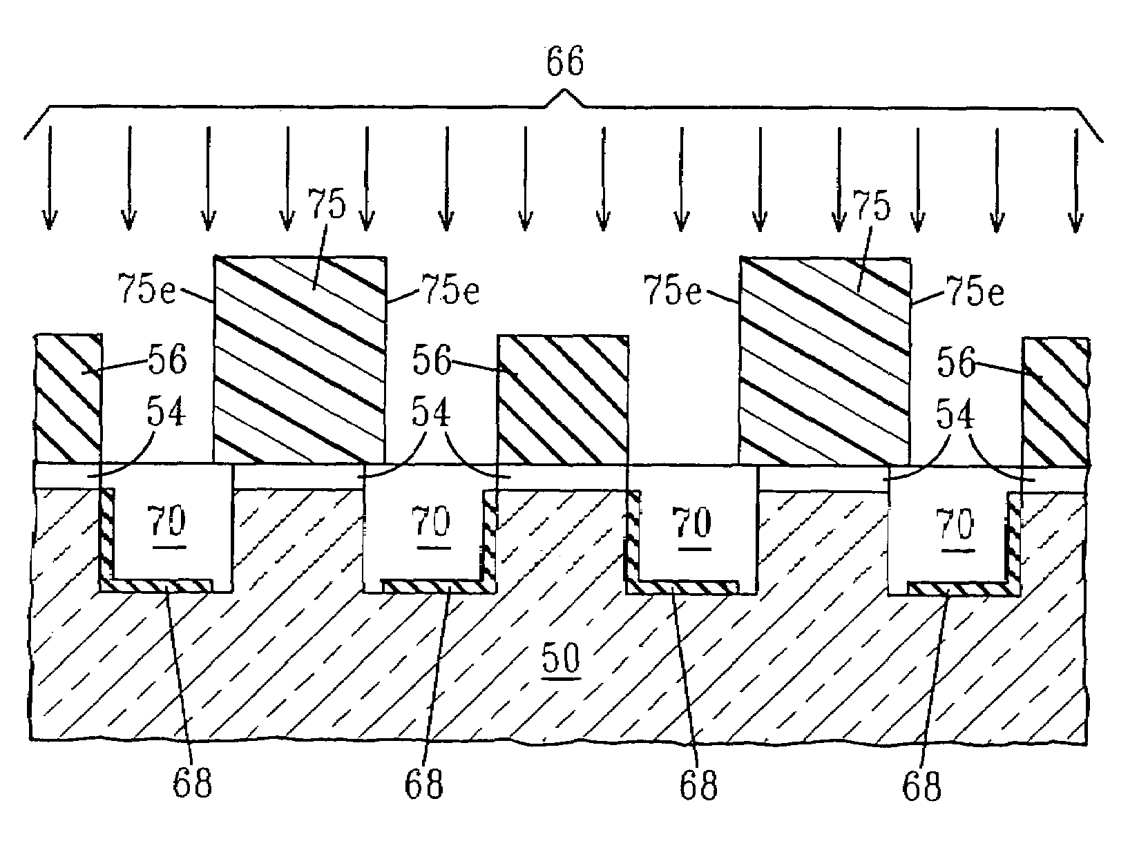
[0028]The plasma nitridation process of the present invention may occur during the formation of the isolation region. In one embodiment, the plasma nitridation process may occur after trench etching, but prior to trench fill. In yet another embodiment of the present invention, the plasma nitridation process occurs after filling the trench with a trench dielectric material. In yet another embodiment of the present invention, a block mask is formed over predetermined active areas of the etched substrate prior to the plasma nitridation process. This embodiment is used in protecting the PFET device area from the plasma nitridation process thereby providing a means to form a PFET device area in which compression stress caused by bird beak formation increases the device performance of the PFET.
[0036]a nitride liner present at least on portions of the sidewalls, said nitride liner protecting the sidewalls of the at least one trench so as to reduce stress in the semiconductor substrate.

Problems solved by technology

This uneven stress may negatively impact some of the devices, while positively affecting other devices present on the semiconductor substrate.
Specifically, stress caused by bird beak formation is known to lead to device degradation for NFET devices and device improvements for PFETs.
In particular, the device drive current and the device on-current can be affected (either negatively or positively) by bird beak formation.

Method used


Image

  • STI stress modification by nitrogen plasma treatment for improving performance in small width devices
  • STI stress modification by nitrogen plasma treatment for improving performance in small width devices
  • STI stress modification by nitrogen plasma treatment for improving performance in small width devices

Examples


Embodiment Construction

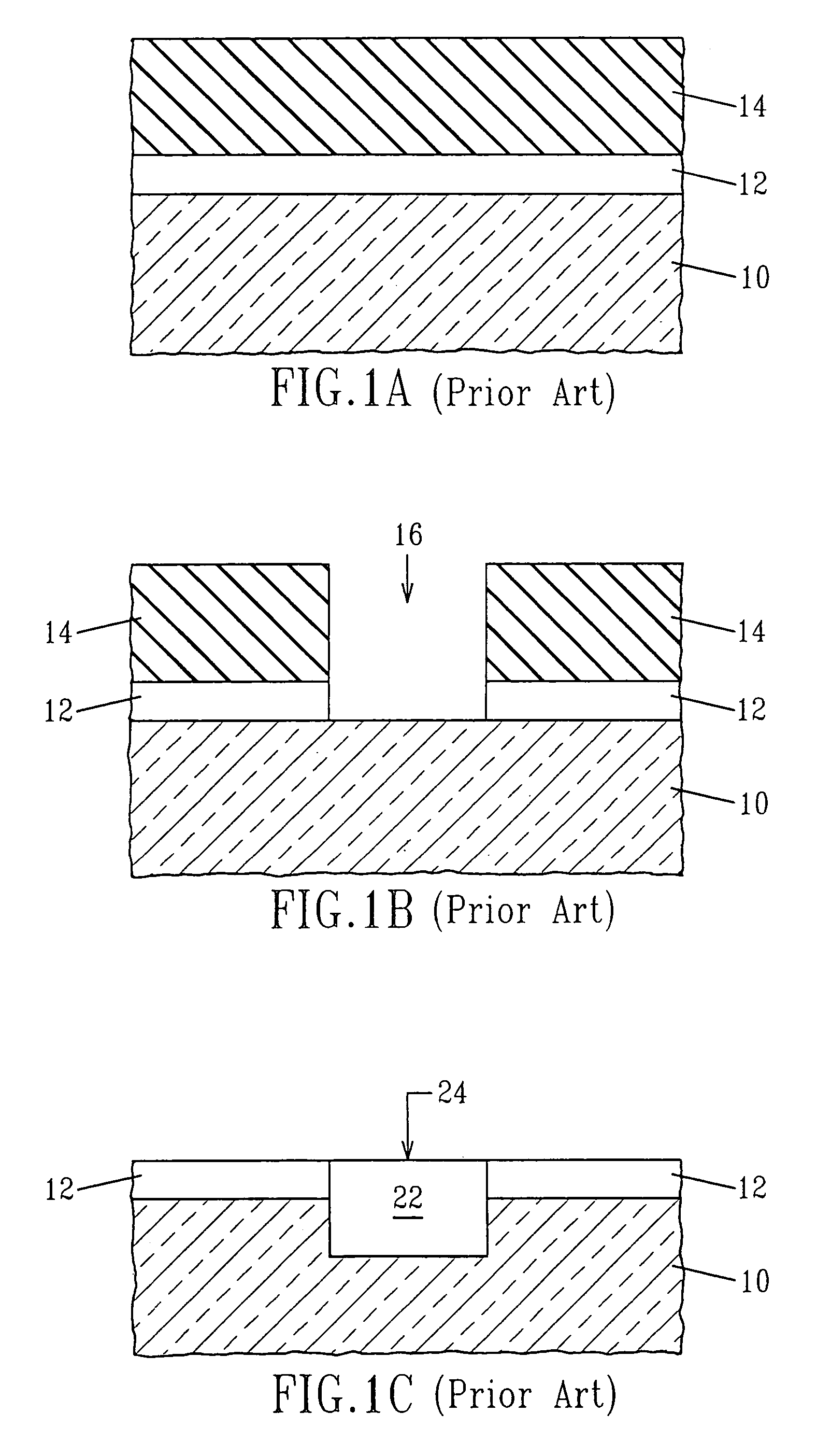
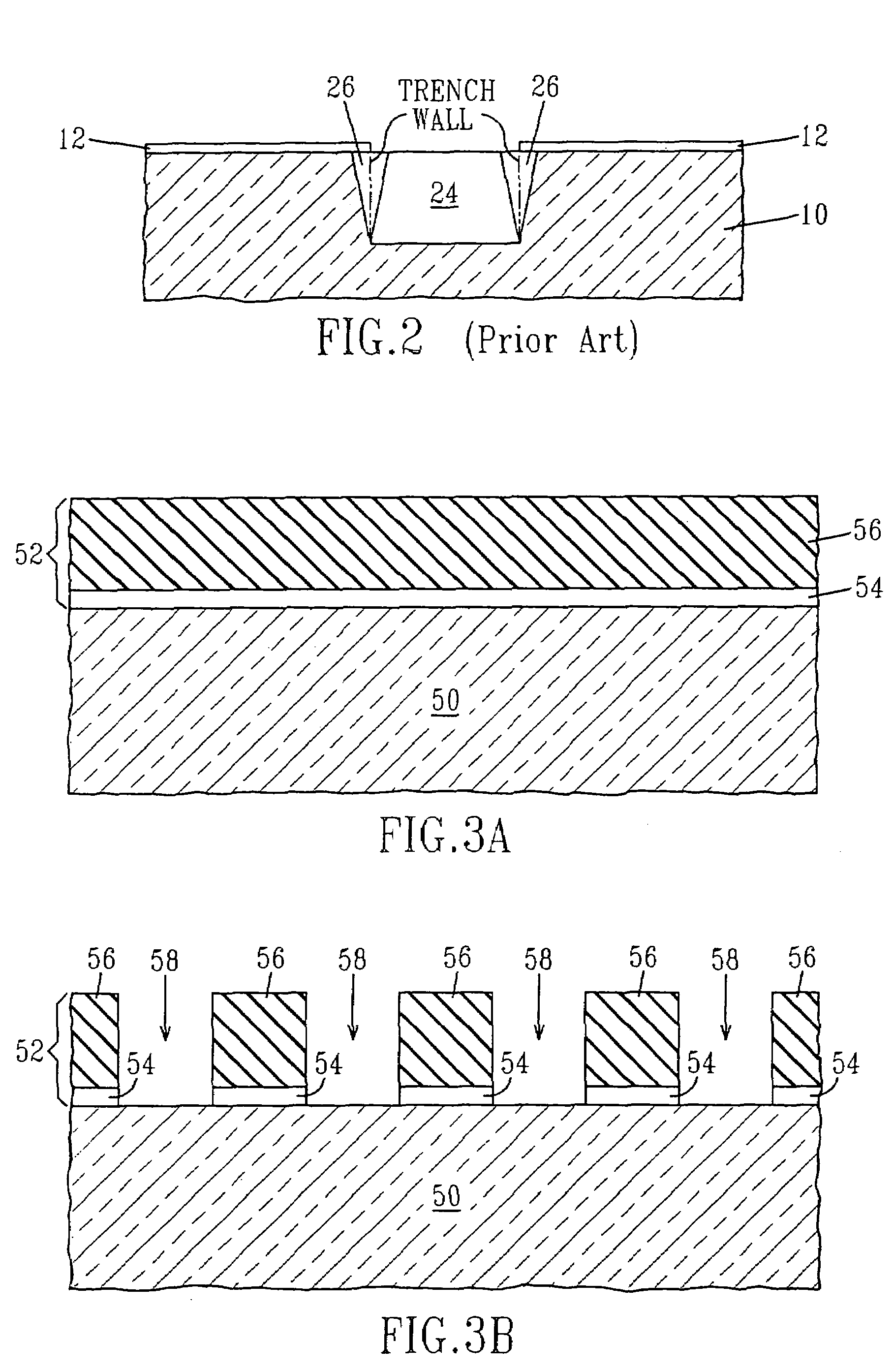
[0042]The present invention, which provides a method for modifying the stress caused by bird beak formation in the isolation regions of small width CMOS devices, will now be described in greater detail by referring to the drawings that accompany the present application. In the drawings representing the present invention, like reference numerals are used in describing like and / or corresponding elements.

[0043]Reference is first made to the embodiment depicted in FIGS. 3A-3E. In this embodiment of the present invention, the trench is subjected to a plasma nitridation process prior to filling the trench with a trench fill material. Specifically, FIG. 3A shows an initial structure of the first embodiment of the present application. In FIG. 3A, there is shown a semiconductor substrate 50 having a material stack 52 located on a surface of the semiconductor substrate 50. Material stack 52 comprises at least a pad oxide 54 and a pad nitride 56. As shown, the pad oxide 54 is located on an upp...


PUM

PropertyMeasurementUnit
thicknessaaaaaaaaaa
widthaaaaaaaaaa
depthaaaaaaaaaa

Abstract

A method for modulating the stress caused by bird beak formation of small width devices by a nitrogen plasma treatment. The nitrogen plasma process forms a nitride liner about the trench walls that serves to prevent the formation of bird beaks in the isolation region during a subsequent oxidation step. In one embodiment, the plasma nitridation process occurs after trench etching, but prior to trench fill. In yet another embodiment, the plasma nitridation process occurs after trench fill. In yet another embodiment, a block mask is formed over predetermined active areas of the etched substrate prior to the plasma nitridation process. This embodiment is used in protecting the PFET device area from the plasma nitridation process thereby providing a means to form a PFET device area in which stress caused by bird beak formation increases the device performance of the PFET.

Description

RELATED APPLICATION[0001]This application is a divisional of U.S. application Ser. No. 10 / 250,047, filed May 30, 2003 now U.S. Pat. No. 6,887,798.DESCRIPTION[0002]1. Field of the Invention[0003]The present invention generally relates to semiconductor processing, and more particularly to a method of fabricating isolation regions, such as shallow trench isolation (STI), in which the stress of the isolation region has been modulated by a nitrogen plasma treatment. The isolation regions created in the present invention, which are particularly useful in small width devices (on the order of about 0.25 μm or less), have substantially little or no bird beaks in the isolation region.[0004]2. Background of the Invention[0005]In the semiconductor industry, it is well known to isolate one or more device regions present on a semiconductor structure using isolation regions such as shallow trench isolation (STI) regions. A standard STI process is shown, for example, in FIGS. 1A-1C. Specifically, p...

Claims


Application Information

Patent Timeline
Patent Type & Authority Patents(United States)
IPC IPC(8): H01L29/72H01L21/318H01L21/762H01L29/10
CPCH01L21/3185H01L21/76237H01L29/1033H01L29/7842H01L21/0217
Inventor DESHPANDE, SADANAND V.DORIS, BRUCE B.RAUSCH, WERNER A.SLINKMAN, JAMES A.
Owner ALSEPHINA INNOVATIONS INC
Why Eureka
Try Eureka