Circular silicon substrates with thin film membranes for electron microscopy

Inactive Publication Date: 2009-01-27
FINCH DUDLEY S
View PDF2 Cites 17 Cited by
  • Summary
  • Abstract
  • Description
  • Claims
  • Application Information

AI Technical Summary

Benefits of technology

[0011]The present invention provides a circular silicon substrate with a thin film membrane for use in transmission electron microscopes, which includes a silicon substrate and a silicon nitride thin film deposited on the silicon substrate. More specifically, it provides a silicon substrate onto which is deposited a silicon nitride thin film as an optical and electron transparent substrate for use i

Problems solved by technology

One of the key differences of this application is the need to control the residual stress in the silicon nitride film so that it exhibits sufficient tensile strength to remain taut without excessive tensile strength that could lead to rupture of the thin film.
Under these conditions however, the silicon nitride films exhibit a very high tensile stress (>1 GPa) and therefore these films are easily frac

Method used


Image

  • Circular silicon substrates with thin film membranes for electron microscopy
  • Circular silicon substrates with thin film membranes for electron microscopy
  • Circular silicon substrates with thin film membranes for electron microscopy

Examples


Embodiment Construction

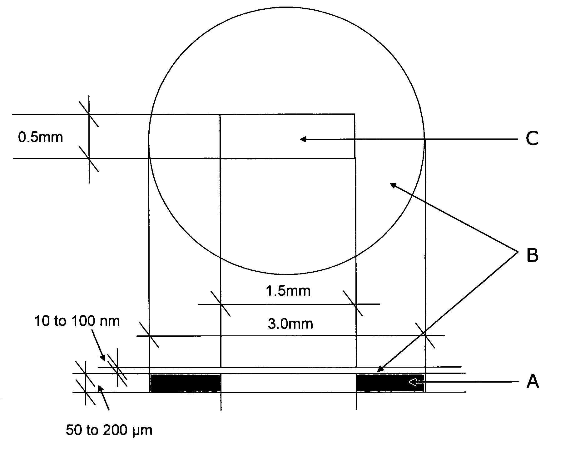
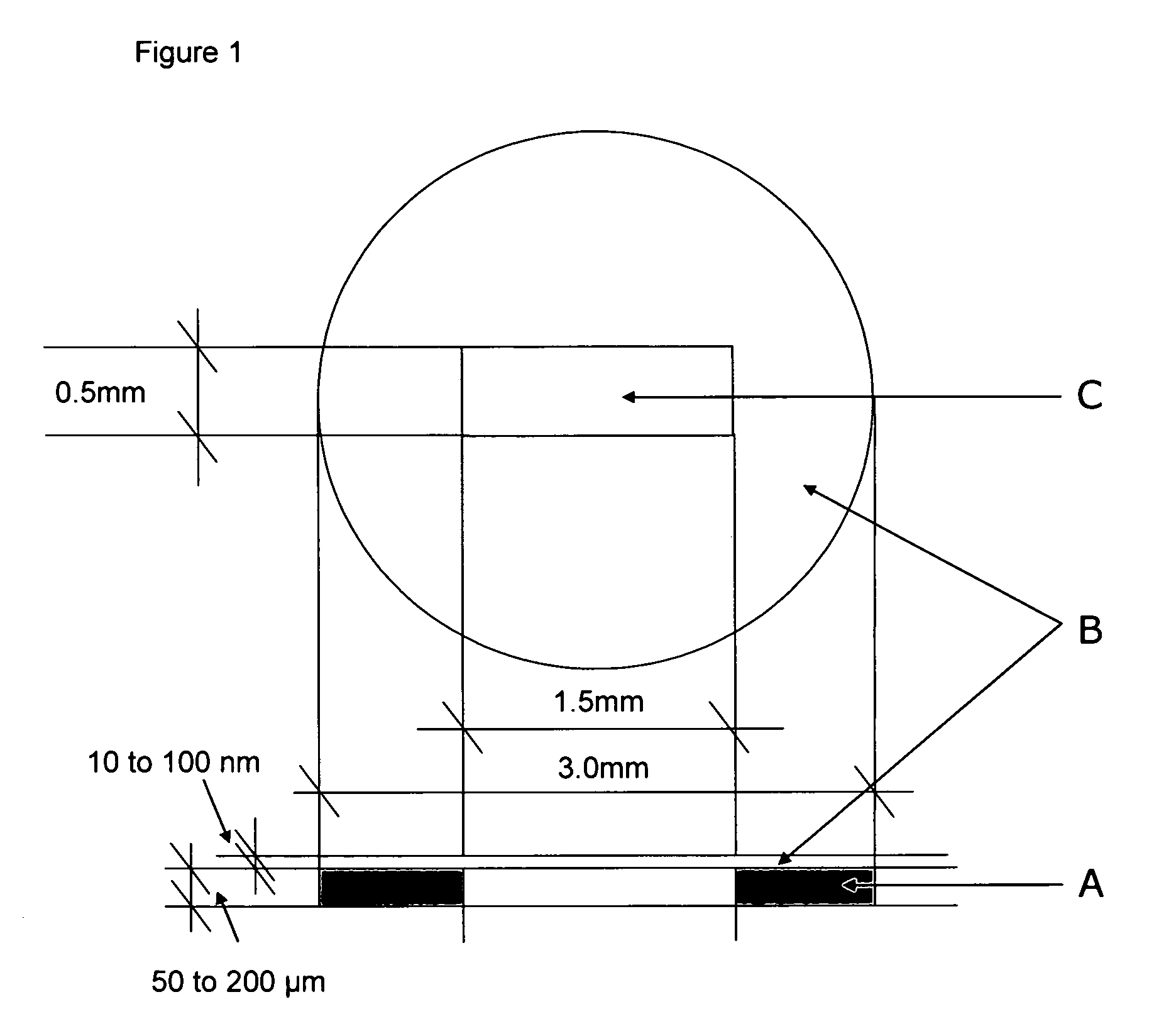
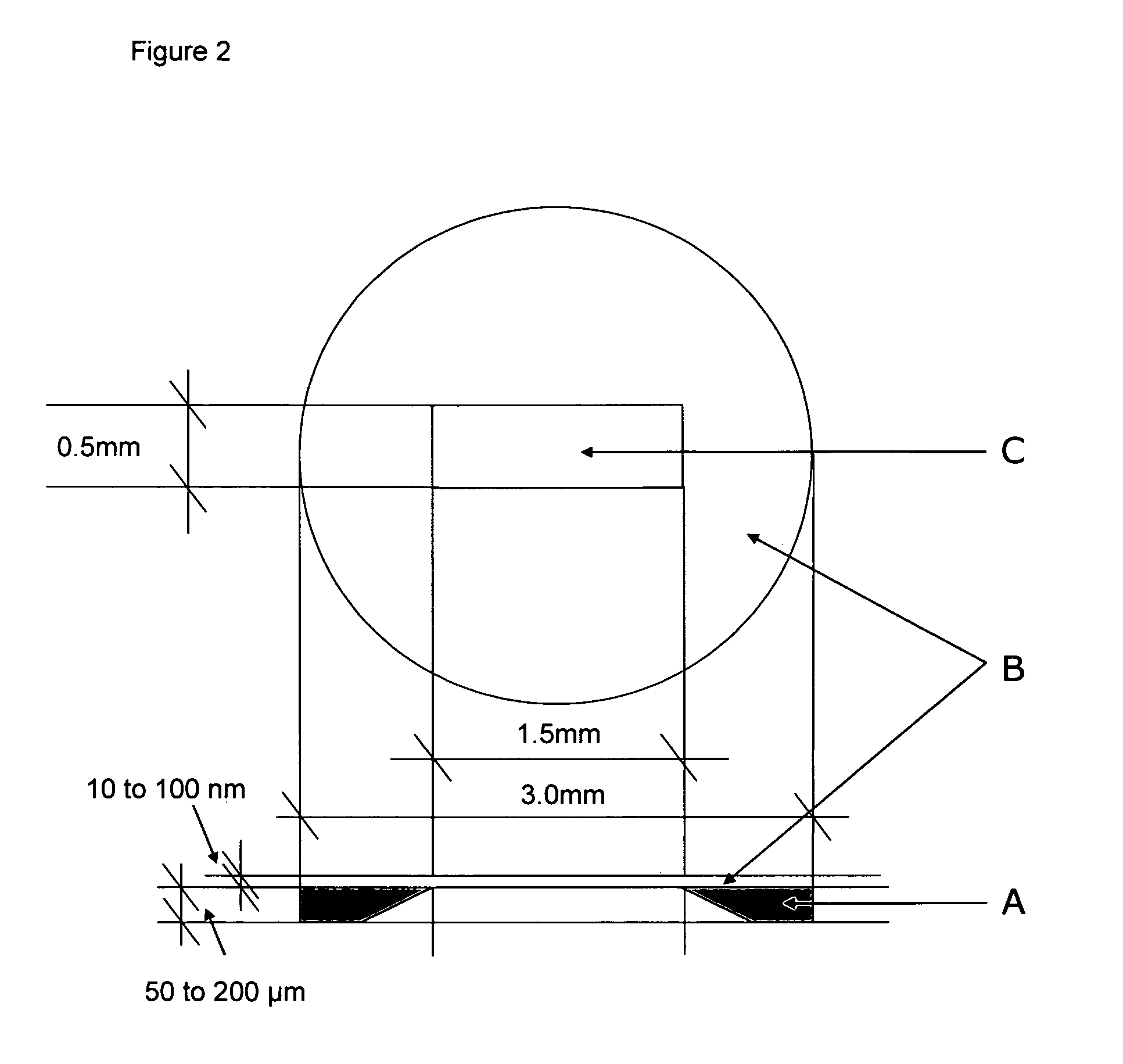
[0018]Transmission electron microscopy is a technique widely used in the disciplines of biological and materials sciences. At its core, it relies on the ability to image through an object following the interaction of electrons with the specimen. This allows the operator to observe a specimen at high spatial resolution for the purpose of identifying composition and structure in relation to a macroscopic property. An example in biological sciences is the study of the chemical synapse of the neuron, whereby transmission electron microscope images of the synapse can be used to understand complex chemical processes in cell-to-cell signaling. An example in the materials science field might be using a transmission electron microscope to image an interface between two dissimilar materials in an attempt to understand the relationship between this structure and some externally measured macroscopic physical property.

[0019]In order to fully utilize the transmission electron microscope, it is im...


PUM

PropertyMeasurementUnit
Thicknessaaaaaaaaaa
Angleaaaaaaaaaa
Shapeaaaaaaaaaa

Abstract

The present invention disclosure relates to the use of a silicon substrate with a thin film membrane as a transparent substrate for the imaging of biological- and material-related specimens using a microscope such as a transmission electron microscope (TEM). More specifically, the present invention relates to an improved substrate design that incorporates the fabrication of a circular shape that allows easier insertion into traditional specimen holders used in TEMs. In addition to an improved shape, the present invention incorporates microscopic surface texture on the gripping surface that assists in handling. The invention also encompasses surface modification techniques for enhanced biocompatibility of the thin film membrane for biomedical applications.

Description

[0001]This patent is based on the previous provisional patent application number 60 / 739,394 filed on 23 Nov. 2005.FIELD OF THE INVENTION[0002]Generally, the present invention relates to the fabrication of a circular silicon substrate with a transparent thin film for the imaging of biological- and material-related samples using a microscope such as a transmission electron microscope (TEM). More specifically, the present invention is an improved substrate design employing fabrication of a circular shape that allows easier insertion into traditional specimen holders used in TEMs. In addition to an improved shape, the present invention incorporates microscopic surface texture on the gripping surface that assists in handling, and also incorporates a modified surface to promote, for example, biological cell adhesion.DESCRIPTION OF RELATED ART[0003]Silicon substrates with thin film membranes made of silicon nitride for example have been utilized in many applications where optical and elect...

Claims


Application Information

Patent Timeline
IPC IPC(8): G01N1/28B01D63/00G01N13/16
CPCH01J37/20H01J37/26H01J2237/20H01J2237/2002H01J2237/2004
Inventor FINCH, DUDLEY SEAN
Owner FINCH DUDLEY S
Why Eureka
Try Eureka