Supercharge Your Innovation With Domain-Expert AI Agents!

Transparent conductor

a transparent conductor and conductor technology, applied in the direction of conductive layers on insulating supports, plastic/resin/waxes insulators, instruments, etc., can solve the problems of difficult to adequately suppress achieve the effect of suppressing the increase or change over time in the electrical resistance of the transparent conductor, excellent wear resistance, and good wear resistan

Inactive Publication Date: 2009-03-24
TDK CORPARATION
View PDF12 Cites 0 Cited by
  • Summary
  • Abstract
  • Description
  • Claims
  • Application Information

AI Technical Summary

Benefits of technology

The present invention provides a transparent conductor that can effectively suppress increase or change over time in its electrical resistance, even in high-humidity environments or under the influence of chemical substances. This is achieved by using a binder with fluorocarbon groups on its side chains. The fluorocarbon groups prevent moisture and chemical substances from entering the conductive layer and infiltrating it, resulting in a dense structure that prevents wear and tear on the conductor surface. The conductor also exhibits excellent wear resistance and water / oil-repelling properties. Overall, the transparent conductor has excellent durability and can be used in various applications such as touch panels and displays.

Problems solved by technology

However, in the case of using a light-transmitting conductive material as described in Japanese Patent Application Laid-open No. 08-78164 or Japanese Patent Application Laid-open No. 11-273874 as a transparent conductor in a touch panel or the like, if this transparent conductor is placed under a high-humidity environment or an atmosphere of a chemical substance, then it tends to be difficult to adequately suppress increase in or change over time in the electrical resistance of the transparent conductor.

Method used


Image

  • Transparent conductor
  • Transparent conductor
  • Transparent conductor

Examples


first embodiment

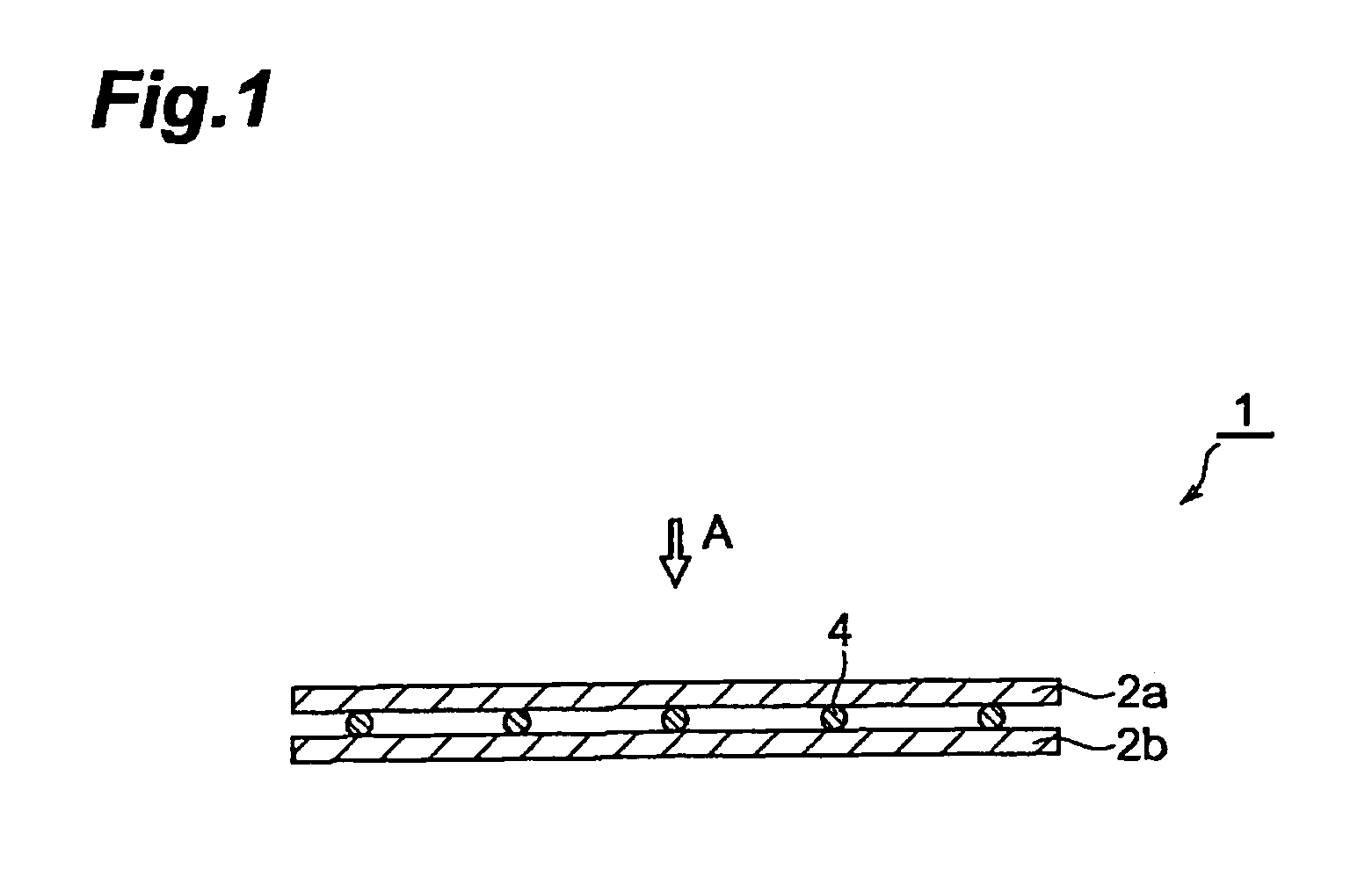
[0034]FIG. 1 is a schematic sectional view showing a touch panel to which one embodiment of a transparent conductor of the present invention is applied. As shown in FIG. 1, the touch panel 1 of the present embodiment comprises a pair of transparent conductors 2a and 2b facing one another, and spacers 4 provided between the pair of transparent conductors.

[0035]In the touch panel 1, the transparent conductor 2a is pressed from the outside A of the transparent conductor 2a, so that the transparent conductor 2a contacts the other transparent conductor 2b and thus a current flows, whereby the position of the point of contact is detected.

Here, a description will be given of the transparent conductor 2a.

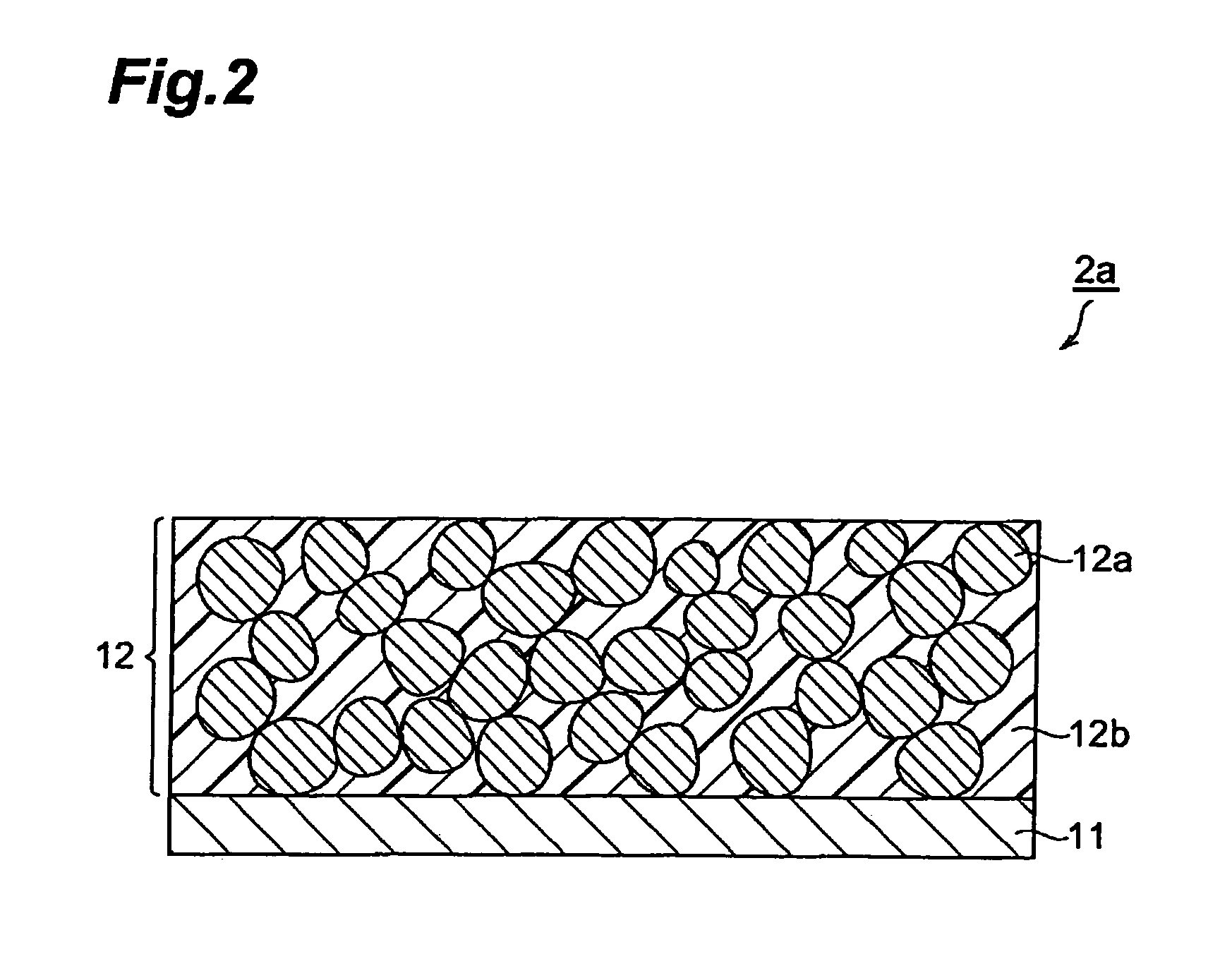
[0036]FIG. 2 is a schematic sectional view showing the transparent conductor 2a. As shown in FIG. 2, the transparent conductor 2a comprises a substrate 11, and a conductive layer 12 containing conductive particles 12a and a cured material 12b of a binder. The transparent conductor 2a, is ...

second embodiment

[0091]Next, a second embodiment of the touch panel of the present invention will be described. Note that component elements the same as or similar to ones in the first embodiment are designated by the same reference numeral as in the first embodiment, and redundant repeated description will be omitted.

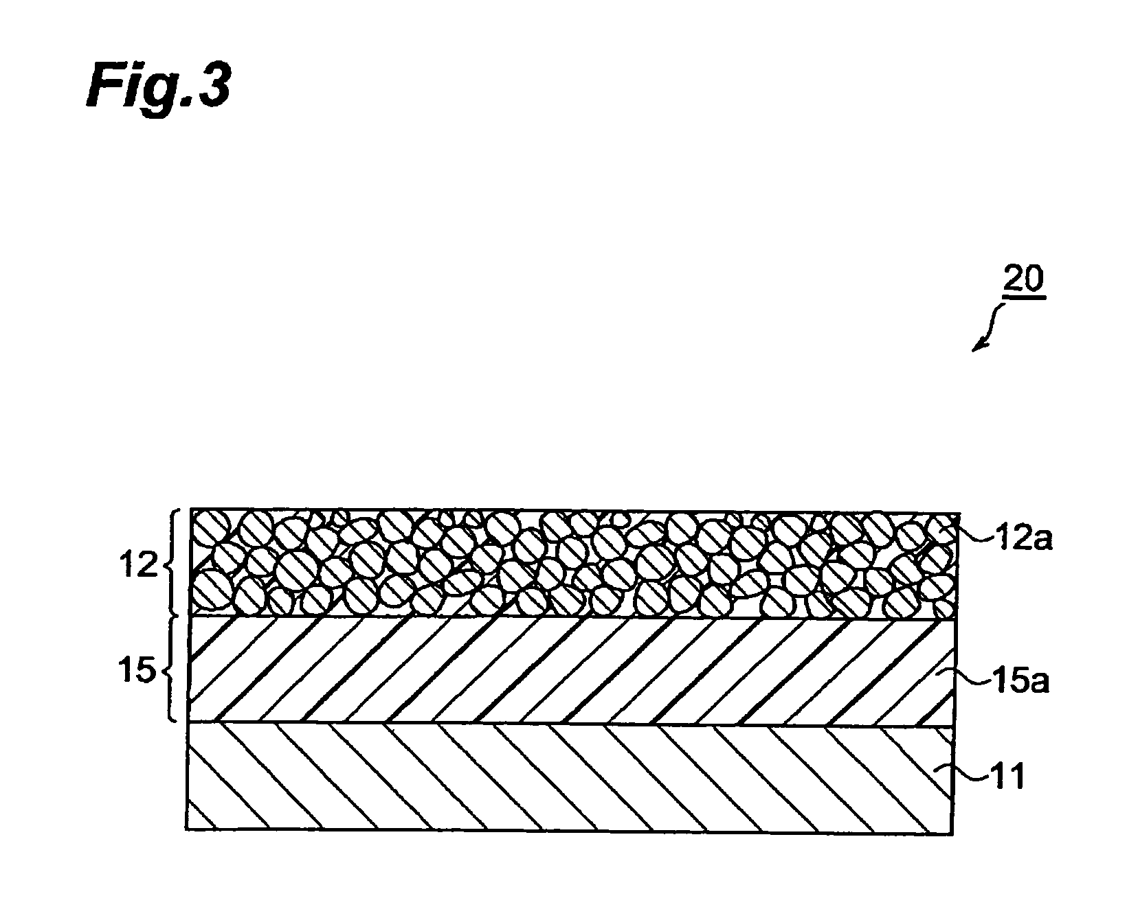
[0092]FIG. 3 is a schematic sectional view showing a transparent conductor used in the second embodiment of the touch panel of the present invention. As shown in FIG. 3, the transparent conductor 20 comprises a substrate 11, a cured material layer 15, and a conductive layer 12 containing conductive particles 12a, the cured material layer 15 and the conductive layer 12 being laminated on the substrate 11 in this order. The conductive particles 12a are packed together in the conductive layer 12; cured material 15a that has penetrated in is present between the conductive particles 12a, the cured material 15a fixing the conductive particles 12a in place.

[0093]As for the transparent conduct...

example 1

[0109]One end of a 10 cm×30 cm polyethylene terephthalate (PET) film (substrate, made by Teijin, thickness 100 μm) was stuck onto a glass baseplate using double sided adhesive tape, thus fixing the substrate onto the glass baseplate.

[0110]Next, 150 parts by mass of the ITO powder (mean particle diameter 30 nm), 50 parts by mass of 2-(perfluorooctyl)ethyl acrylate (monomer, made by Daikin Fine Chemical Laboratory, trade name: R-1820), 20 parts by mass of polyethylene glycol diacrylate (made by Shin-Nakamura Chemical Corporation, trade name: A-400), 5 parts by mass of dipentaerythritol hexaacrylate (other monomer, made by Shin-Nakamura Chemical Corporation, trade name: A-DPH), 25 parts by mass of an acrylic polymer (average molecular weight approximately 100,000 average of 50 acryloyl groups and average of 25 triethoxysilane groups per molecule), and 1 part by mass of a UV polymerization initiator (made by Ciba Specialty Chemicals, trade name: IRGACURE 907) were dispersed in 30 parts ...


PUM

PropertyMeasurementUnit
glass transition pointaaaaaaaaaa
mean particle diameteraaaaaaaaaa
specific surface areaaaaaaaaaaa

Abstract

The present invention provides a transparent conductor comprising a substrate, and a conductive layer containing conductive particles and a cured material of a binder, wherein the binder has at least one substituent selected from the group comprising substituents represented by undermentioned general formula (1) to (4) on side chains thereofF—(CF2)n—  (1)F—(CF2CF2O)m—  (2)F—(CF2CF2CF2O)p—  (3)In formula (1) to (3), n, m and p each represents a positive integer.

Description

BACKGROUND OF THE INVENTION[0001]1. Field of the Invention[0002]The present invention relates to a transparent conductor.[0003]2. Related Background Art[0004]A panel switch such as a touch panel is generally constituted from a pair of transparent electrodes facing one another, and spacers sandwiched between the pair of transparent electrodes or else dot spacers printed on a conductive surface of one of the pair of transparent electrodes. With such a panel switch, upon one of the transparent electrodes being pressed, this transparent electrode contacts the other transparent electrode so that a current flows, whereby the position of the point of contact is detected. Transparent conductors are used as such transparent electrodes, and as such transparent conductors there are ones in which a sputtered film is deposited as a conductive layer on a substrate, and ones in which a conductive layer comprising conductive particles and a binder is formed on a substrate.[0005]However, if such a t...

Claims


Application Information

Patent Timeline
Patent Type & Authority Patents(United States)
IPC IPC(8): B32B27/32B32B27/00B32B5/16H01B3/44
CPCB32B27/00H01B1/22Y10T428/26Y10T428/25Y10T428/31511Y10T428/3154H01B1/20H01B5/14
Inventor YASUDA, NORIYUKIHIKIDA, KOICHIYAMADA, CHIEKO
Owner TDK CORPARATION
Features
  • R&D
  • Intellectual Property
  • Life Sciences
  • Materials
  • Tech Scout
  • Unparalleled Data Quality
  • Higher Quality Content
  • 60% Fewer Hallucinations
Learn More