Semiconductor chip electrical connection structure

a technology of semiconductor chip and electrical connection, applied in the direction of semiconductor device details, semiconductor/solid-state device details, electrical apparatus, etc., can solve the problems of inability to print stencils, difficulty in reducing size, and difficulty in putting solder material on contact pads of circuit boards through such small stencil openings, so as to simplify fabrication processes and interface integration, and effectively provide outward electrical extension

Active Publication Date: 2009-04-07
PHOENIX PRECISION TECH CORP
View PDF4 Cites 13 Cited by
  • Summary
  • Abstract
  • Description
  • Claims
  • Application Information

AI Technical Summary

Benefits of technology

[0011]In light of the above prior-art drawbacks, a primary objective of the present invention is to provide a semiconductor chip electrical connection structure, wherein a circuit build-up process can be directly performed on conductive bumps formed on electrode pads of a semiconductor chip so as to accomplish electrical connection between the semiconductor chip and an external electronic element, such that fabrication processes of a semiconductor chip carrier and a semiconductor package are integrated, thereby providing better flexibility responsive to the requirements for clients and simplifying the fabrication processes and interface integration.
[0012]Another objective of the present invention is to provide a semiconductor chip electrical connection structure, which can effectively provide outward electrical extension for a semiconductor chip via simplified fabrication processes in response to the requirement of high integration of integrated circuits.
[0013]Still another objective of the present invention is to provide a semiconductor chip electrical connection structure, which can prevent problems of poor electricity and defective process reliability resulted from conventional electrical connection between a semiconductor chip and a circuit board by using a flip-chip and wire-bonding technique.
[0014]A further objective of the present invention is to provide a semiconductor chip electrical connection structure, which can simplify a connection manner between a semiconductor chip and a semiconductor chip carrier to reduce the fabrication processes and the cost, and also improve the electrical capability and reliability of an electrical connection interface of the semiconductor chip.
[0015]In accordance with the foregoing and other objectives, the present invention proposes a semiconductor chip electrical connection structure, comprising: a plurality of electrode pads formed on a surface of a semiconductor chip, wherein the semiconductor chip is attached via another surface thereof to a carrier; a plurality of conductive bumps respectively formed on the electrode pads, and exposed from a dielectric layer applied on the semiconductor chip and the carrier; and a plurality of electrical connection pads formed on the dielectric layer and electrically connected to the conductive bumps exposed from the dielectric layer, so as to provide outward electrical extension for the semiconductor chip via the electrical connection pads. Accordingly, for the semiconductor chip electrical connection structure in the present invention, conductive bumps are firstly formed on electrode pads of a semiconductor chip, and then a dielectric layer is applied on the semiconductor chip and partly removed to expose the conductive bumps. Subsequently, electrical connection pads (comprising at least electrical connection pads sized slightly larger than the conductive bumps) are formed on the dielectric layer by a circuit patterning process, such that the electrical connection pads are electrically connected to the conductive bumps exposed from the dielectric layer. This allows the highly integrated chip to be electrically extended outwardly via the conductive bumps formed on the electrode pads and via the electrical connection pads electrically connected to the conductive bumps under a condition of fine circuits and a fine pitch between the adjacent electrode pads. As a result, a circuit build-up process can be subsequently performed on the electrical connection pads to form a circuit build-up structure electrically connected to the semiconductor chip, so as to effectively provide outward electrical extension for the semiconductor chip.
[0016]Compared with the conventional wire-bonding or flip-chip semiconductor packaging technique, the semiconductor chip electrical connection structure in the present invention can advantageously provide direct outward electrical connection for the semiconductor chip via the semiconductor chip electrical connection structure formed thereon (such as electrode pads, conductive bumps and electrical connection pads) and via a circuit build-up structure formed by a build-up process or conductive elements. Thus, the electrical capability and electrical connection reliability of a connection interface of the semiconductor chip can be assured, and fabrication processes of a semiconductor chip carrier and a semiconductor package can be integrated. This thereby provides better flexibility responsive to the requirements for clients, and simplifies the semiconductor fabrication processes and interface integration, as well as prevents the problems in the prior art resulted from electrical connection between a semiconductor chip and a semiconductor chip carrier and caused by a molding process.

Problems solved by technology

This not only causes a positional alignment problem during subsequently forming pre-solder bumps, but also requires decrease of the size of stencil openings in the stencil printing technique, thereby leading to difficulty in depositing the solder material on the contact pads of the circuit board through such small stencil openings.
As a result, the stencil printing technique would have low yield and becomes infeasible.
Moreover, the stencil cost would be increased due to reduction in the pad size and pad pitch, making the fabrication cost raised.
Furthermore, with the pad pitch being decreased, a contact area between the insulating protective layer and the circuit board is reduced, and thus adhesion therebetween becomes weakened.
This further causes difficulty in fabricating fine-pitch pre-solder bumps and achieving good electrical connection.
Such method not only increases the fabrication processes and cost, but also raises the risk of degrading the reliability during fabrication.
Moreover, according to the requirement of IC integration, the circuit size or the size and pitch of electrode pads and contact pads become gradually smaller, such that when electrical connection is to be subsequently formed for such fine circuits and such fine-pitch electrode pads and contact pads, precise positional alignment and fabrication are required but are actually very difficult to achieve.
Besides, when either the flip-chip packaging technique or the wire-bonding packaging technique is used, fabrication of the circuit board and packaging of the semiconductor chip must adopt different fabrication machines and processes, thereby making the fabrication processes complicated and the fabrication cost increased.
However, in practice, the mold may be limited by the design of the semiconductor package, thereby causing undesirable inaccuracy of size of a mold cavity and clamping positions, and a problem such as infirm clamping and so on.
Moreover, when the resin material is injected into the mold, the encapsulant may easily flash to the surface of the circuit board.
Such flashes not only impair the surface smoothness and the appearance of the semiconductor package, but also may contaminate bond pads on the circuit board for subsequently forming solder balls thereon, thereby degrading the electrical connection quality of the semiconductor package, and severely deteriorating the fabrication quality and product reliability of the semiconductor package.
The fabrication processes involve different manufacturers (including the semiconductor chip carrier manufacture and the semiconductor package manufacturer), and thus are relatively complicated and cause difficulty in interface integration.
If the clients wish to alter the function design, the associated changes and interface integration are even more complicated, thereby not providing sufficient flexibility in design alternation and economical benefits.

Method used


Image

  • Semiconductor chip electrical connection structure
  • Semiconductor chip electrical connection structure
  • Semiconductor chip electrical connection structure

Examples


Embodiment Construction

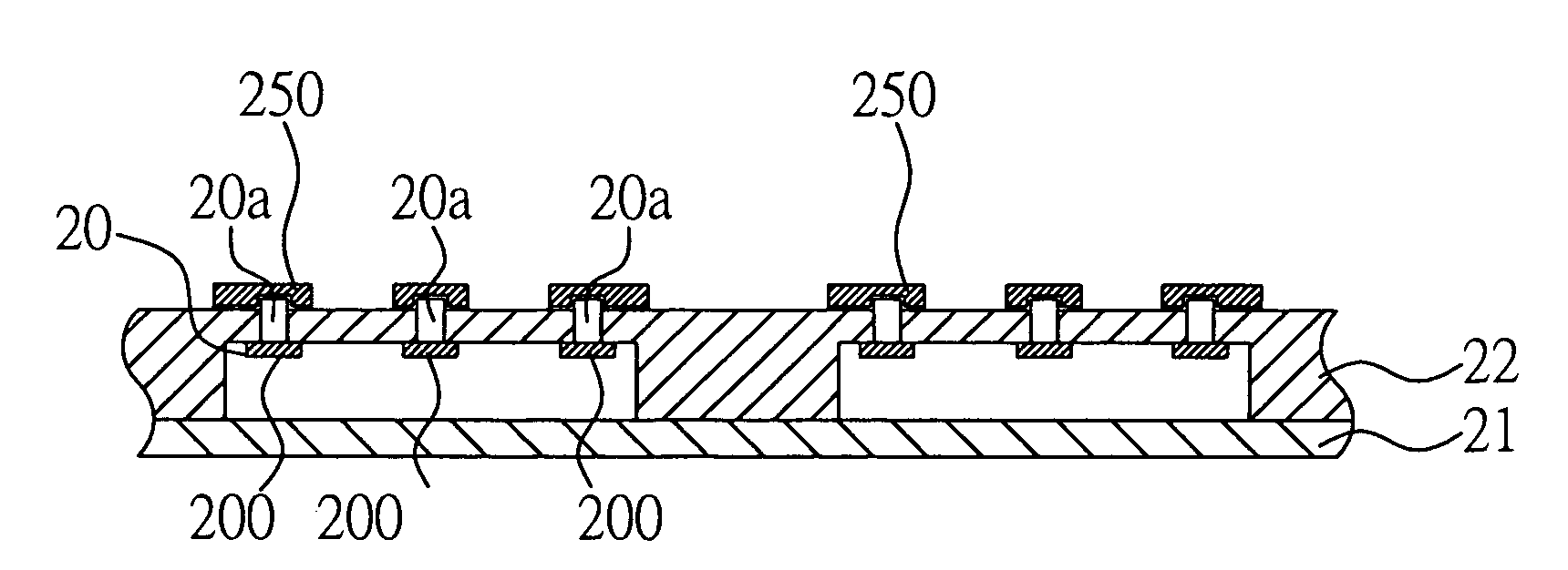
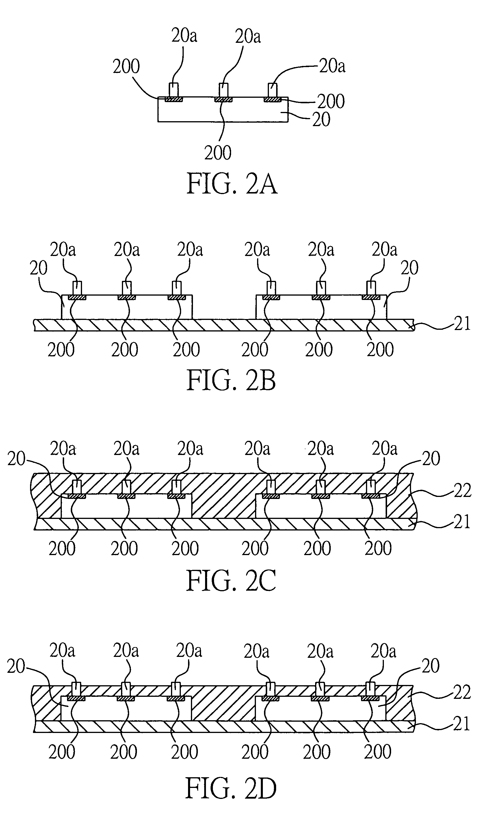
[0021]Preferred embodiments of a semiconductor chip electrical connection structure proposed in the present invention are described in detail as follows with reference to FIGS. 2A to 2G and FIGS. 3A to 3C.

[0022]FIGS. 2A to 2G are cross-sectional schematic diagrams showing procedural steps of a method for fabricating a semiconductor chip electrical connection structure according to the present invention.

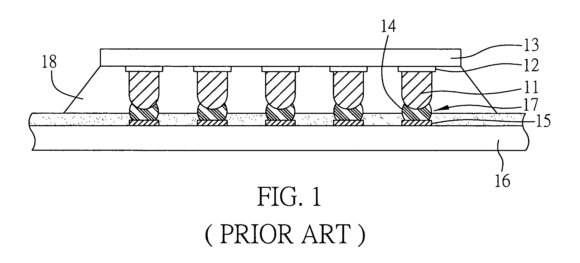
[0023]As shown in FIG. 2A, one or more chips 20 each having electrode pads 200 thereon are provided, with a plurality of conductive bumps 20a being formed on the electrode pads 200 respectively. The conductive bump 20a can be made of a conductive metal selected from the group consisting of copper (Cu), gold (Au), silver (Ag), tin (Sn), nickel (Ni) and palladium (Pd), or comprises a plurality of layers made of the foregoing metals. In practice, the conductive bump 20a is preferably made of, but not limited to, copper (Cu). Further, the conductive bumps 20a can be formed by a technique ...


PUM


Abstract

A semiconductor chip electrical connection structure includes electrode pads formed on a surface of a semiconductor chip, wherein the semiconductor chip is mounted via another surface thereof on a carrier; a plurality of conductive bumps formed on the electrode pads respectively, and exposed from a dielectric layer applied on the semiconductor chip and the carrier; and a plurality of electrical connection pads formed on the dielectric layer and electrically connected to the conductive bumps exposed from the dielectric layer so as to provide outward electrical extension for the semiconductor chip via the electrical connection pads.

Description

FIELD OF THE INVENTION[0001]The present invention relates to semiconductor chip electrical connection structures, and more particularly, to a conductive structure for providing electrical extension from electrode pads of a semiconductor chip.BACKGROUND OF THE INVENTION[0002]Along with evolution of the semiconductor packaging technology, various types of packages for semiconductor devices have been developed. For instance, Ball Grid Array (BGA) employs an advanced semiconductor packaging technique, which is characterized by disposing a semiconductor chip on a front side of a substrate, and mounting a plurality of array-arranged solder balls on a back side of the substrate via a self-alignment technique. This arrangement allows more input / output (I / O) connections to be accommodated on the same unit of area of a semiconductor chip carrier to satisfy the requirement for highly integrated chips, and the entire package unit can be bonded and electrically connected to an external printed c...

Claims


Application Information

Patent Timeline
Patent Type & Authority Patents(United States)
IPC IPC(8): H01L23/48H01L21/44
CPCH01L24/19H01L23/5389H01L2224/0401H01L2224/20H01L2224/211H01L2924/01029H01L2924/01046H01L2924/01079H01L2924/01082H01L2924/14H01L2924/15311H01L21/561H01L2924/01033H01L2924/01047H01L2224/16225H01L2224/32225H01L2224/73204H01L2224/04105H01L2924/00H01L2224/12105
Inventor HSU, SHIH-PING
Owner PHOENIX PRECISION TECH CORP
Why Eureka
Try Eureka