Ball grid array package-to-board interconnect co-design apparatus

a co-design and package technology, applied in the direction of solid-state devices, printed circuit components, basic electric elements, etc., can solve the problems of enlarge the package and board thickness, fail to meet the requirements of the application, and the cost of the device is not practical or cost-effective, so as to improve the signal transmission and avoid reflection and radiation, the effect of superior electromagnetic shielding

Active Publication Date: 2009-04-07
TAHOE RES LTD
View PDF3 Cites 30 Cited by
  • Summary
  • Abstract
  • Description
  • Claims
  • Application Information

AI Technical Summary

Benefits of technology

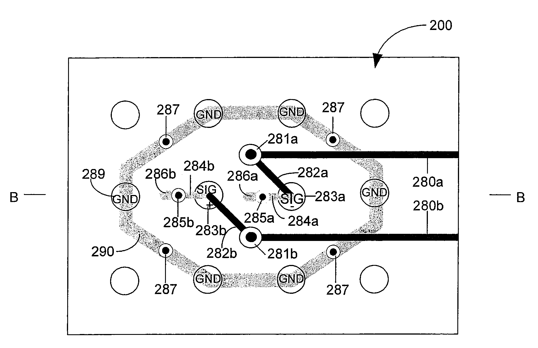
[0010]The present invention provides a package-board co-design methodology that preserves the signal integrity of high-speed signals passing from semiconductor packages to application PCBs. The present invention further provides an architecture of interconnects between package and PCB that enhances the signal propagation, minimizes parasitic levels, and decreases electromagnetic interference from adjacent high frequency signals. The invention results in devices with superior signal quality and EMI shielding properties with enhanced capability for carrying data stream at multiple-gigabit per second bit-rates.
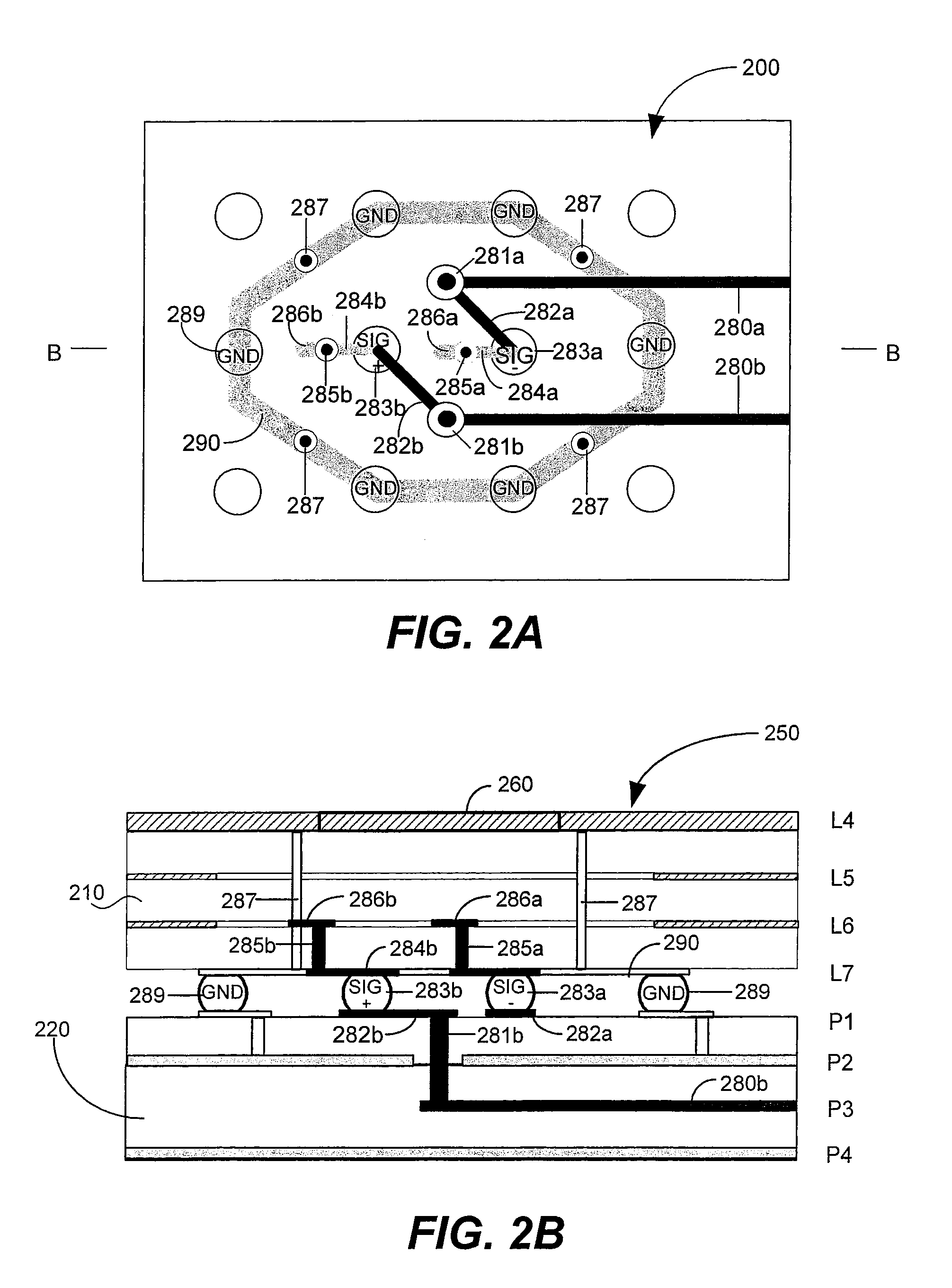
[0011]The BGA package-to-board co-design accomplishes routing signals from the semiconductor device package to the PCB, for example in high-speed FPGA and ICs and other applications. The co-design accounts for the via-to-BGA pad transition and BGA ball-to-PCB interconnection. The approach effectively takes packaging and PCB as an integral part of a high-speed integrated circuit design process and enables packaging and PCB designers to work interactively from packaging and board material selection and layer stack-up to signal routing and interconnection at and between the package and board
[0013]An electromagnetic interference (EMI) shielding cavity is formed by solid ground / power planes, BGA balls, metal strips, and via array. Within this shielding cavity, a metal plane cut or clearance is enforced within the vicinity of a signal ball or balls in order to achieve the goals of parasitic capacitance reduction and impedance control. These efforts then enhance signal transmission, avoid reflection and radiation, and provide superior electromagnetic shielding.
[0014]The invention also allows the design of high-performance, multiple-gigabit per second capable IC packages made from low-cost organic material.

Problems solved by technology

However BGA packaging brings new challenges to the packaging designers, particularly in high-speed IC applications, where the effects of electromagnetic interference (EMI) become extremely important, and BGA I / O densities exasperate this problem.
Signal integrity is another important issue for packages and boards emerging from high-speed transceivers in high-end FPGAs and ICs.
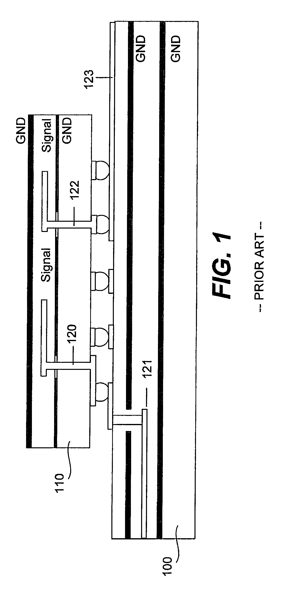
This approach enlarges the package and board thickness and has been proved neither practical nor cost effective.

Method used


Image

  • Ball grid array package-to-board interconnect co-design apparatus
  • Ball grid array package-to-board interconnect co-design apparatus
  • Ball grid array package-to-board interconnect co-design apparatus

Examples


Embodiment Construction

[0023]Reference will now be made in detail to specific embodiments of the invention. Examples of the specific embodiments are illustrated in the accompanying drawings. While the invention will be described in conjunction with these specific embodiments, it will be understood that it is not intended to limit the invention to such specific embodiments. On the contrary, it is intended to cover alternatives, modifications, and equivalents as may be included within the spirit and scope of the invention as defined by the appended claims. In the following description, numerous specific details are set forth in order to provide a thorough understanding of the present invention. The present invention may be practiced without some or all of these specific details. In other instances, well known process operations have not been described in detail in order not to unnecessarily obscure the present invention.

[0024]Introduction

[0025]As a result of the emerging field of high-speed (e.g., multigiga...


PUM


Abstract

A package-board co-design methodology preserves the signal integrity of high-speed signals passing from semiconductor packages to application PCBs. An optimal architecture of interconnects between package and PCB enhances the signal propagation, minimizes parasitic levels, and decreases electromagnetic interference from adjacent high frequency signals. The invention results in devices with superior signal quality and EMI shielding properties with enhanced capability for carrying data stream at multiple-gigabit per second bit-rates.

Description

CROSS REFERENCE TO RELATED APPLICATION[0001]This application is a divisional of prior application Ser. No. 11 / 292,685 filed on Dec. 1, 2005, now pending.BACKGROUND OF THE INVENTION[0002]1. Field of the Invention[0003]The present invention relates to signal transition from ball grid array (BGA) packages to printed circuit board (PCB) intended for high-speed applications. More specifically, the present invention relates to package-board co-design methodology and optimal interconnect architecture between package and printed circuit board layers.[0004]2. Description of Related Art[0005]The ball grid array (BGA) package offers a number of advantages relative to other, older package types (e.g., quad flat pack (QFP) and pin grid array (PGA)), including small size, high input / output (I / O) pin count, improved electrical performance, low profiles, and good yields. The packages can be constructed with a substrate that can be either single or multi-layer. Substrates are fabricated with plastic...

Claims


Application Information

Patent Timeline
Patent Type & Authority Patents(United States)
IPC IPC(8): H01L23/48
CPCH01L23/49838H01L23/552H05K1/0243H01L2223/6622H01L2223/6627H01L2223/6638H01L2924/1903H01L2924/19051H01L2924/3011H05K1/0298H05K2201/0191H05K2201/09718H05K2201/10734H01L2924/0002H01L2924/00H01L2224/16227
Inventor TAO, YUMINGLONG, JON M.PANNIKKAT, ANILKUMAR RAMAN
Owner TAHOE RES LTD
Why Eureka
Try Eureka