
System and method for floating-substrate passive voltage contrast

a passive voltage contrast and floating substrate technology, applied in the direction of individual semiconductor device testing, semiconductor/solid-state device testing/measurement, instruments, etc., can solve the problems of complex methods, extensive pre-processing, and the need for grounding the body of a soi device while performing pvc analysis

Inactive Publication Date: 2009-04-28
NAT TECH & ENG SOLUTIONS OF SANDIA LLC
View PDF17 Cites 16 Cited by
  • Summary
  • Abstract
  • Description
  • Claims
  • Application Information

AI Technical Summary

Benefits of technology

[0012]The present invention relates to a method for measuring passive voltage contrast (PVC) on a device side of a semiconductor die which comprises the steps of maintaining the device side of the semiconductor die in an electrically-floating condition without any ground electrical connection; directing a beam of charged particles at the device side of the semiconductor die, and scanning the beam of charged particles over the device side of the semiconductor die; and detecting a secondary particle emission from the device side of the semiconductor die.

Problems solved by technology

Electrically grounding the body of a SOI device while performing PVC analysis requires extensive pre-processing.
However, this also requires extensive pre-processing as described in U.S. Pat. No. 6,991,946.
However, in a packaged device, access of the electron beam to the body requires grinding through the substrate from the bottom side, and then etching through the oxide layer to expose the body.
This method is complicated and requires a specialized dual-beam system to provide the two pulsed charged particle beams.

Method used


Image

  • System and method for floating-substrate passive voltage contrast
  • System and method for floating-substrate passive voltage contrast
  • System and method for floating-substrate passive voltage contrast

Examples


Embodiment Construction

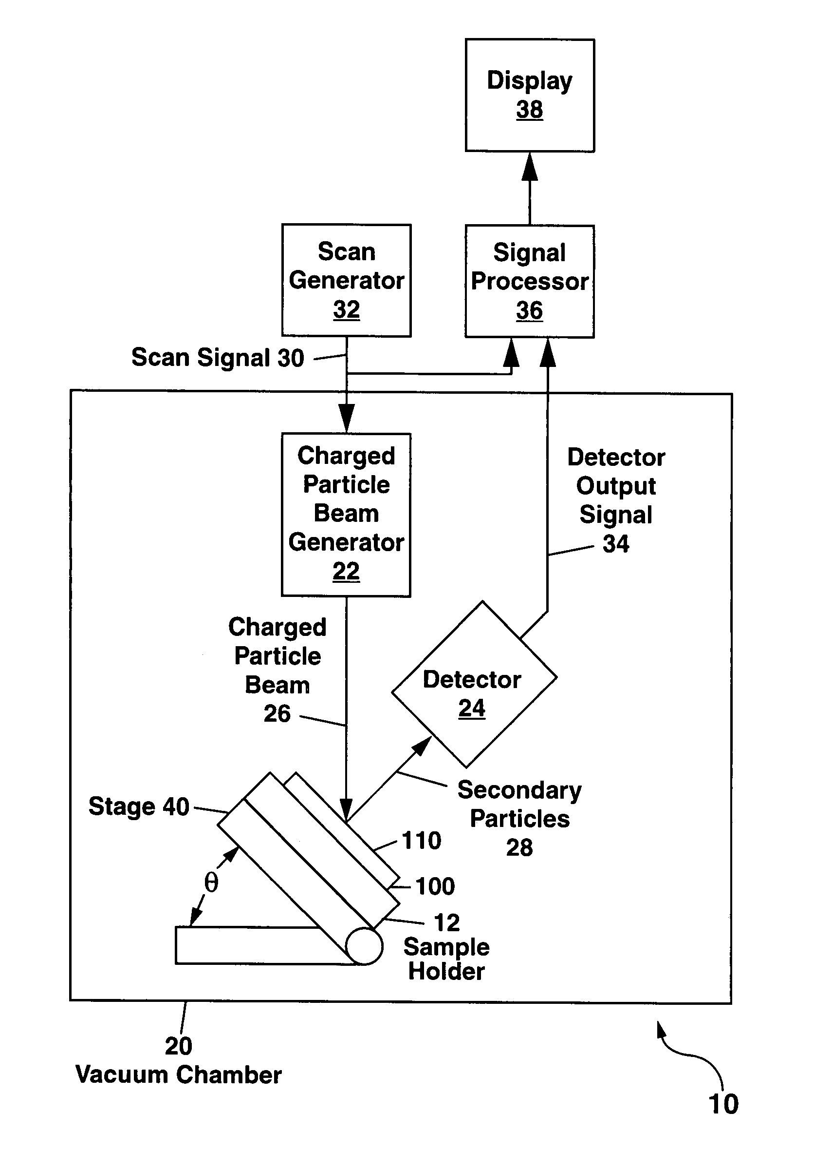
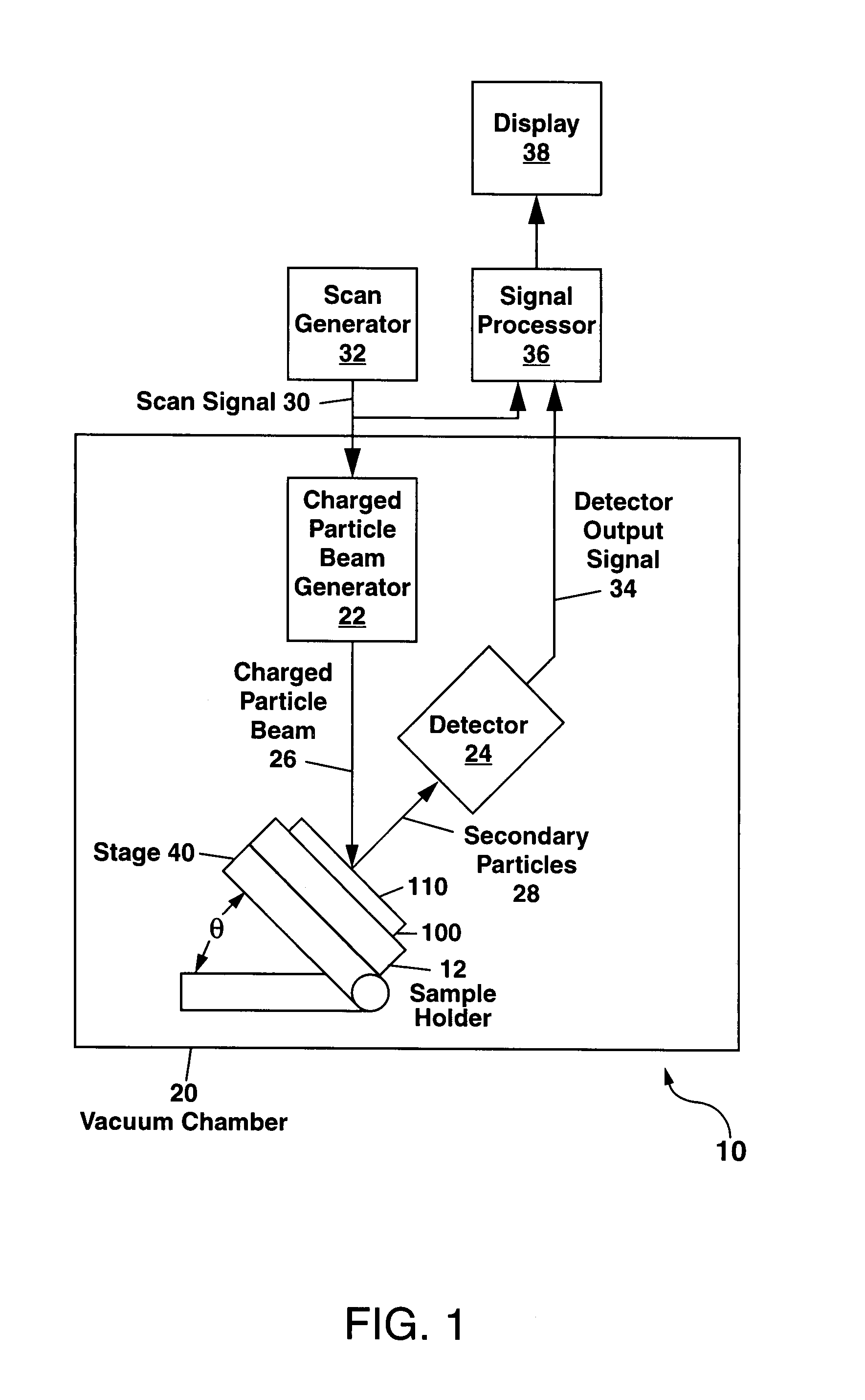
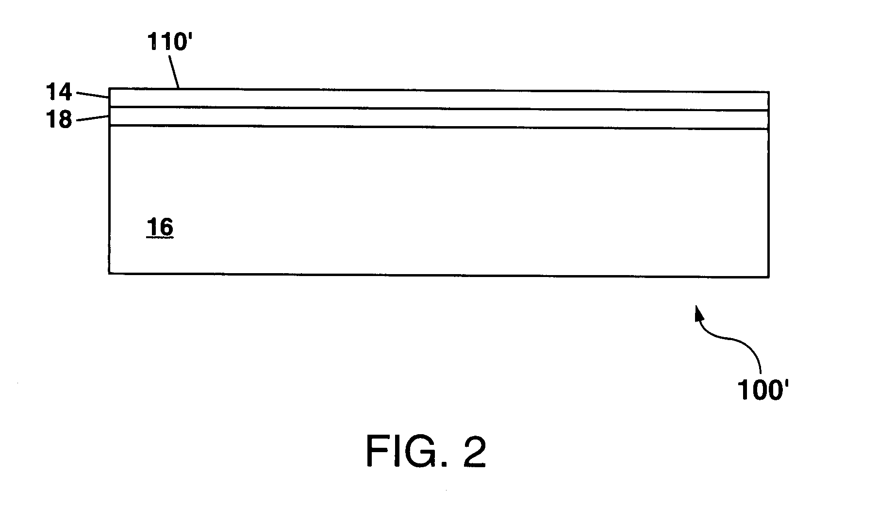
[0036]FIG. 1 shows a schematic diagram of a floating-substrate PVC system 10 of the present invention which is referred to hereinafter as a FSPVC system 10. The term “floating-substrate” as used herein refers to a semiconductor substrate 100 (also termed a semiconductor die) having a device side 110 on which an IC is formed comprising a plurality of interconnected transistors, with the device side 110 being maintained in an electrically-floating condition without any ground electrical connection (i.e. without any connection to a ground electrical potential either directly, or through a power supply). In the case of a bulk semiconductor substrate 100, the substrate itself must be electrically-floating since the device side 110 is an integral part of the substrate 100. In the case of a SOI substrate 100′, the device side 110′ is electrically isolated from the remainder of the substrate so that only the device side 110′ need be electrically floating.

[0037]To provide a “floating substra...


PUM

PropertyMeasurementUnit
currentaaaaaaaaaa
energyaaaaaaaaaa
energyaaaaaaaaaa

Abstract

A passive voltage contrast (PVC) system and method are disclosed for analyzing ICs to locate defects and failure mechanisms. During analysis a device side of a semiconductor die containing the IC is maintained in an electrically-floating condition without any ground electrical connection while a charged particle beam is scanned over the device side. Secondary particle emission from the device side of the IC is detected to form an image of device features, including electrical vias connected to transistor gates or to other structures in the IC. A difference in image contrast allows the defects or failure mechanisms be pinpointed. Varying the scan rate can, in some instances, produce an image reversal to facilitate precisely locating the defects or failure mechanisms in the IC. The system and method are useful for failure analysis of ICs formed on substrates (e.g. bulk semiconductor substrates and SOI substrates) and other types of structures.

Description

GOVERNMENT RIGHTS[0001]This invention was made with Government support under Contract No. DE-AC04-94AL85000 awarded by the U.S. Department of Energy. The Government has certain rights in the invention.FIELD OF THE INVENTION[0002]The present invention relates in general to systems and methods for detecting defects and failure mechanisms in semiconductor integrated circuits (ICs), and in particular to a floating-substrate passive voltage contrast (PVC) failure analysis system and method that can be used to detect defects and failure mechanisms in ICs formed on bulk semiconductor or silicon-on-insulator (SOI) substrates, and other types of structures.BACKGROUND OF THE INVENTION[0003]Passive voltage contrast (PVC) is a failure analysis tool which can be used to detect defects and failure mechanisms in complementary metal oxide semiconductor (CMOS) ICs such as a gate oxide breakdown. In the PVC method, a scanning electron microscope (SEM) can be used to direct a beam of electrons onto th...

Claims


Application Information

Patent Timeline
Patent Type & Authority Patents(United States)
IPC IPC(8): G01R31/305G01N23/00G01R31/26
CPCG01R31/307
Inventor JENKINS, MARK W.COLE, JR., EDWARD I.TANGYUNYONG, PAIBOONSODEN, JERRY M.WALRAVEN, JEREMY A.PIMENTEL, ALEJANDRO A.
Owner NAT TECH & ENG SOLUTIONS OF SANDIA LLC
Learn More