Semiconductor device, electronic device having the same, and driving method of the same

a technology of electromagnetic field and semiconductor device, applied in the field of digital circuit, can solve the problems of sequential malfunction of subsequent digital circuits, circuits that do not operate normally, and high possibility of malfunction

Inactive Publication Date: 2009-05-05
SEMICON ENERGY LAB CO LTD
View PDF24 Cites 40 Cited by
  • Summary
  • Abstract
  • Description
  • Claims
  • Application Information

AI Technical Summary

Benefits of technology

[0038]According to the invention, a digital circuit can be operated normally by storing in advance a difference between a potential of a signal which is actually inputted to the digital circuit and a potential which is required to operate the digital circuit normally, and by providing a correcting unit in the digital circuit which adds the potential difference to the potential of the signal which is actually inputted to

Problems solved by technology

In this case, the digital circuit does not operate normally, leading to a high possibility of a malfunction.
Further, it can cause a sequential malfunction in the subsequent digital circuit.
In this case, the digital circuit does not operate normally, leading to a high possibility of a malfunction.
Further, it can cause a sequential malfunction in the subsequent digital circuit.
However, when the binary potentials VDD′ and VSS′ of the input signal IN are in the relations of VDD′VSS respectively, the output signal OUT having a desired potential is not obtained, thus the inverter may not operate normally.
Therefore, the output signal OUT having a desired potential can not be obtained and the digital circuit does not function normally.
A potential of the input signal supplied from a circuit or a wiring of a prior stage is not always an appropriate value for the digital circuit to operate normally.
However, a high-speed operation of the semiconductor device is frequently hindered by using the level shifter, because level shifters generally have problems in that the speed of rising and dropping of the potential of the output signal is low as eac

Method used


Image

  • Semiconductor device, electronic device having the same, and driving method of the same
  • Semiconductor device, electronic device having the same, and driving method of the same
  • Semiconductor device, electronic device having the same, and driving method of the same

Examples


embodiment mode 1

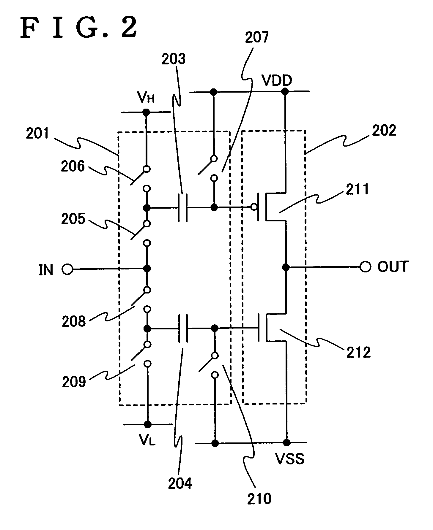
[0077]In this embodiment mode, the specific configuration and operation of an inverter as an example of the digital circuits of the invention are described.

[0078]FIG. 2 shows the configuration of an inverter of this embodiment mode. Reference numeral 201 denotes a correcting unit and 202 denotes a circuit element group.

[0079]The correcting unit 201 comprises a first capacitor 203, a second capacitor 204, switches 205 to 207 for controlling the supply of a potential to the first capacitor 203, and switches 208 to 210 for controlling the supply of a potential to the second capacitor 204.

[0080]The switch 205 controls the supply of a potential of an input signal to the first electrode of the first capacitor 203. The switch 206 controls the supply of a power supply potential VH on the high potential side to the first electrode of the first capacitor 203. The switch 207 controls the supply of a power supply potential VDD to the second electrode of the capacitor 203.

[0081]Meanwhile, the sw...

embodiment mode 2

[0108]In this embodiment mode, the configuration of an inverter as an example of the digital circuits of the invention is described, which is different from the configuration shown in Embodiment Mode 1.

[0109]FIG. 5 shows the configuration of the inverter of this embodiment mode. Reference numeral 301 denotes a correcting unit and 302 denotes a circuit element group.

[0110]The correcting unit 301 comprises a first capacitor 303, a second capacitor 304, a switch 305 for controlling the supply of a power supply potential VDD to the first capacitor 303, and a switch 306 for controlling the supply of a power supply potential VSS to the second capacitor 304.

[0111]Although the power supply potential VDD is supplied to the second electrode of the first capacitor 303 by the switch 305 in this embodiment mode, the invention is not limited to this. Alternate potentials may be supplied to the second electrode of the first capacitor 203 in place of VDD, and the potential to be supplied may be adj...

embodiment mode 3

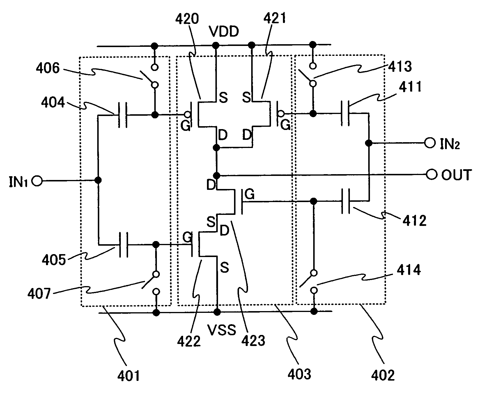
[0133]In this embodiment mode, the configuration of an NAND as an example of the digital circuits of the invention is described.

[0134]The NAND in this embodiment mode which is shown in FIG. 7 comprises a first correcting unit 401, a second correcting unit 402 and a circuit element group 403.

[0135]The first correcting unit 401 comprises a first capacitor 404, a second capacitor 405, a switch 406 for controlling the supply of a power supply potential VDD to the first capacitor 404, and a switch 407 for controlling the supply of a power supply potential VSS to the second capacitor 405.

[0136]The second correcting unit 402 comprises a third capacitor 411, a fourth capacitor 412, a switch 413 for controlling the supply of a power supply potential VDD to the third capacitor 411, and a switch 414 for controlling the supply of the power supply potential VSS to the fourth capacitor 412.

[0137]The circuit element group 403 comprises two p-channel transistors 420 and 421 and two n-channel transi...


PUM


Abstract

A digital circuit which can operate normally regardless of binary potentials of an input signal is provided. A semiconductor device comprising a correcting unit and one or a plurality of circuit elements, the correcting unit including a first capacitor, a second capacitor, a first switch, and a second switch, wherein the first electrode of the first capacitor is connected to an input terminal, the supply of a first potential to the second electrode of the first capacitor is controlled by the first switch, the supply of a second potential to the second electrode of the second capacitor is controlled by the second switch, and a potential of the second electrode of the first capacitor or a potential of the second electrode of the second capacitor is supplied to the one or the plurality of circuit elements.

Description

BACKGROUND OF THE INVENTION[0001]1. Field of the Invention[0002]The present invention relates to a digital circuit which operates in accordance with a digital signal, and more particularly to a semiconductor device having one or a plurality of the digital circuits and a driving method thereof[0003]2. Description of the Related Art[0004]A logic circuit processing a digital signal (hereinafter referred to as a digital circuit) is configured with one or a plurality of logic elements as a basic unit. The logic element is the one which provides one output corresponding to one or a plurality of inputs. Examples of the logic elements include an inverter, an AND, an OR, a NOT, a NAND, a NOR, a clocked inverter, a transmission gate and the like.[0005]The logic element is configured with one or a plurality of circuit elements such as a transistor, a resistor and a capacitor. By operating the plurality of the circuit elements in accordance with a digital signal which is inputted to the logic e...

Claims


Application Information

Patent Timeline
IPC IPC(8): H03K5/08G11C7/00H03K19/017H03K19/0185
CPCH03K19/01728H03K19/01855G11C7/00
Inventor KIMURA, HAJIME
Owner SEMICON ENERGY LAB CO LTD
Why Eureka
Try Eureka