Class D analog-to-digital converter

a technology of analog-to-digital converter and mixed-signal semiconductor, which is applied in the direction of code conversion, transmission system, instruments, etc., can solve the problems of difficult implementation of adc's designed in the traditional way, achieve medium-to-high resolution, and solve the problem of solving a new problem, so as to reduce the number of circuits, high speed of the new transistor, and high performance in one chip

Active Publication Date: 2009-05-05
TEXAS INSTR INC
View PDF10 Cites 26 Cited by
  • Summary
  • Abstract
  • Description
  • Claims
  • Application Information

AI Technical Summary

Benefits of technology

[0010]The present invention provides a circuit and architecture for an analog-to-digital signal conversion (ADC) that make use of modern IC semiconductor process technology advantages such as the high speed of the new transistors (e.g. deep-submicron MOSFET), and that reduce the number of circuits such as amplifiers and particularly analog switches. The new ADC is very compact, low-power and still delivers high performance in one chip. In the case of a PC board level or system level application where more than one chip would be used to implement the architecture, the reduction of the number of components is again useful for reducing cost and board space. Fewer components generally also reduce the effects of stray parasitic capacitances present in the devices, circuit routing and connection nodes.

Problems solved by technology

However, the solution has also presented a new problem.
Because of the migration towards high density, smaller minimum feature size transistor technologies, ADC's designed in the traditional ways are harder to implement, particularly to achieve medium-to-high resolution.
However, they involve much analog circuitry or in the case of the sigma-delta, there is also a massive digital filter circuit, taking up much die area.
Moreover, the design of the analog circuit sub-blocks is becoming very difficult on the small geometry size processes, say, 65 nm MOS process.
However, analog switches are very difficult to turn-off completely in the small-geometry technologies due to leakage current which adds undesirable stray charge to the capacitors in the circuit sub-block.
Because there are so many analog switches needed in the traditional ADC architectures, it is not practical to design each switch specially (e.g. bootstrap the switch) to overcome their limitations.
The other sub-blocks, such as high gain amplifiers in the ADC's, are also harder to design in the new processes.
So the existing ADC's which rely on these sub-blocks to perform really well, are now very difficult to design to meet performance specifications needed by the overall system applications.
So the ADC becomes relatively large and consumes much power.
The resistive or reference ladder with which the input signal amplitude is compared to, also consumes much power if it is designed to be a stiff, constant reference.
A drawback of this methodology is that element 1 is an asynchronous sigma-delta modulator and it also has inherent harmonic distortion.
Yet further, the post-processing digital section, a decimation filter, to turn the modulated pulses into binary data and to do some out-of-band noise removal, is typically large.
Therefore, an ADC based on this scheme is still quite large and consumes a fair amount of power.

Method used


Image

  • Class D analog-to-digital converter
  • Class D analog-to-digital converter
  • Class D analog-to-digital converter

Examples


Embodiment Construction

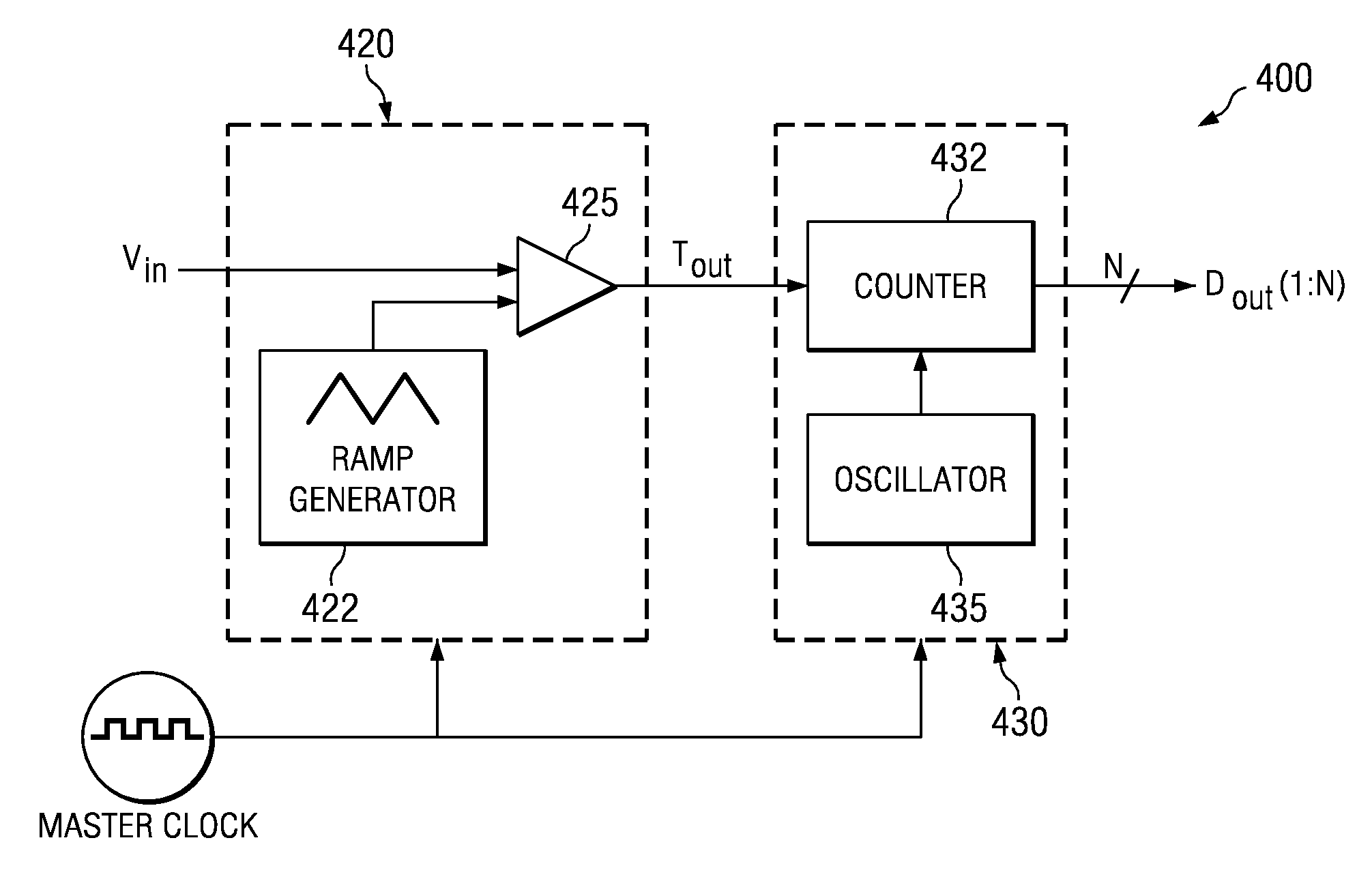
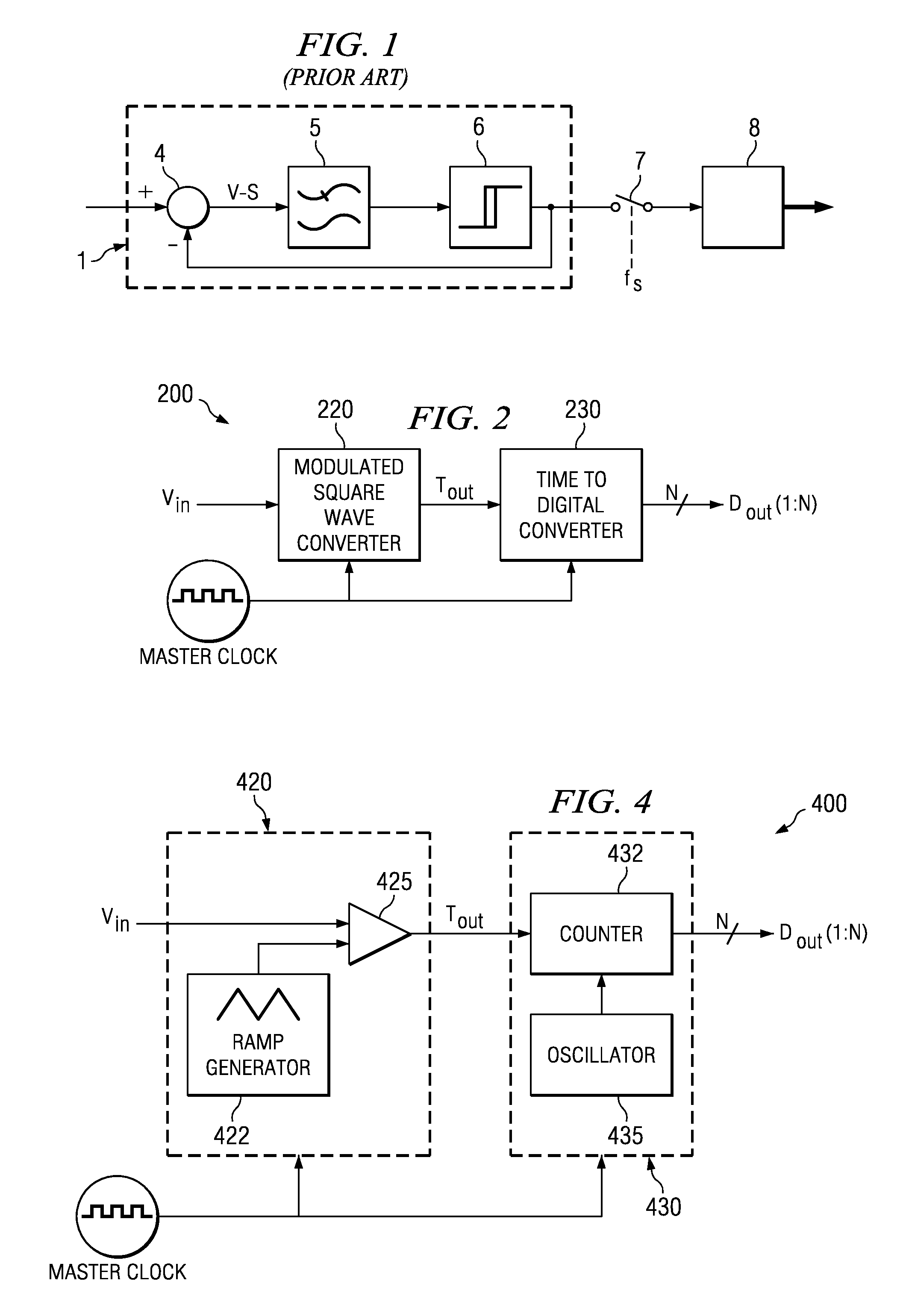
[0021]FIG. 1 is discussed above in the Background of the Invention section of this document and the reader is assumed familiar with the principles of that discussion. For the ADC in this application, instead of quantizing an analog signal in the voltage domain, the analog signal is converted into the time domain (e.g. the time duration of the created pulses corresponds to the amplitude of the analog signal), and then the time domain pulses' widths are sampled (measured) and turned into digital bits which are directly correlated to the voltage amplitude of the original analog signal. As noted in the Background section, the prior art of Engel Roza has a modulation scheme that does have any clocking, forcing a need for extra circuitry, such a sampling circuit, special filtering, decimation and additional timing circuit to align signals from the modulation section to the subsequent circuitry. In contrast, the ADC in this application uses a different modulation scheme that does not need ...


PUM


Abstract

A new analog-to-digital (ADC) circuit and architecture and the corresponding method of implementation are provided. The analog input signal is converted into a modulated pulse stream such as by a pulse-width-modulation scheme. The time-duration width of the pulses are measured by a TDC (time-to-digital converter) and converted to a digital binary representation that is directly correlated with the voltage amplitude of the analog input signal. The circuit implementation is substantially free of switches and circuit issues such as associated with sigma-delta and switched-capacitor techniques for ADC's.

Description

CROSS-REFERENCES TO RELATED APPLICATIONS[0001]Not Applicable.STATEMENT REGARDING FEDERALLY SPONSORED RESEARCH OR DEVELOPMENT[0002]Not Applicable.FIELD OF THE INVENTION[0003]The present embodiments relate to mixed-signal semiconductor circuits such as on a chip (IC) or to circuits with discrete components such as on a printed circuit board (PCB) and are more particularly directed to an analog-to-digital converter (ADC) circuit and architecture.BACKGROUND OF THE INVENTION[0004]Electronic systems often include ADC's as a basic building block in order to convert analog input signals to its digital bit representation for use with digital signal processors, memory, digital filters, and CPU's. With today's high density integration process technologies, such as nanometer CMOS, it is possible and easier to process and manipulate digital signals than analog, particularly when the power supply voltage range is low because digital bits can better overcome signal to noise issues. However, the so...

Claims


Application Information

Patent Timeline
Patent Type & Authority Patents(United States)
IPC IPC(8): H03M1/50
CPCG04F10/005H03M1/504
Inventor FOREJT, BRETT
Owner TEXAS INSTR INC
Why Eureka
Try Eureka