Imaging apparatus and method for manufacturing the same

a technology of imaging apparatus and manufacturing method, which is applied in the field of imaging apparatus, can solve the problems of increasing the number of processes, increasing the cost, and affecting the accuracy of semiconductor imaging devices, so as to facilitate the size and thickness reduction of imaging apparatuses, increase the mechanical strength of the three-dimensional substrate, and facilitate the effect of reducing the size and thickness

Active Publication Date: 2009-05-19
PANASONIC CORP
View PDF7 Cites 6 Cited by
  • Summary
  • Abstract
  • Description
  • Claims
  • Application Information

AI Technical Summary

Benefits of technology

[0010]In order to solve the above-mentioned conventional problems, it is an object of the present invention to provide an imaging apparatus that achieves thickness reduction and an improvement in workability, and allows air circulation between the exterior and a cavity enclosed by a semiconductor imaging device and an optical filter, while suppressing the entry of foreign matter from the exterior into the cavity via an airflow caused by expansion / contraction of air.
[0012]According to this configuration, for example, in a heating process for fabricating an imaging apparatus, when gas (air) existing in a cavity expands / contracts, air circulation is performed only through a passage having a non-linear structure, and thus the entry of foreign matter from the exterior can be prevented reliably. This can prevent a phenomenon in which foreign matter entering from the exterior causes a so-called flaw in an image that deteriorates the image, and thus can reduce the occurrence of a failure in a process resulting from thickness reduction.
[0016]Preferably, the three-dimensional substrate has such a low light transmittance with respect to a region sensitive to light reception by the semiconductor imaging device that substantially no unwanted signal is generated. According to this configuration, with regard to the achievement of higher sensitivity of semiconductor imaging devices that is pursued along with the size reduction of imaging apparatuses, an influence of disturbance light can be reduced in an imaging apparatus, thus suppressing a functional deterioration of the imaging apparatus when used in portable equipment that is used outdoors frequently. Moreover, even when the imaging apparatus is used in so-called skeleton type portable equipment, which is future portable equipment that itself has a translucent housing, the entry of light entering from the periphery can be prevented reliably, making it possible to prevent a deterioration of an image with reliability.
[0017]Furthermore, preferably, the air passages are located at a position axisymmetric with respect to the opening in the three-dimensional substrate. According to this configuration, anisotropy caused at the time of heating after a transparent plate is bonded to a three-dimensional substrate can be reduced, and thus it is possible to prevent a decrease in the flatness of a flat surface on which a semiconductor imaging device is mounted. This facilitates the thickness reduction of imaging apparatuses.
[0019]According to this manufacturing method, since an optical filter is fixed by bonding with respect to a three-dimensional substrate, the mechanical strength of the three-dimensional substrate is increased, and thus, in a later process, it becomes easier to secure the accuracy of, for example, a required flatness at the time of mounting a semiconductor imaging device. Moreover, by subsequently sealing the semiconductor imaging device, the entry of foreign matter into a cavity between the semiconductor imaging device and the optical filter can be prevented reliably. This prevents a phenomenon in which foreign matter in an imaging apparatus causes a flaw, thereby facilitating the size and thickness reduction of imaging apparatuses.

Problems solved by technology

Because of this, in a heating process for bonding or joining, the flatness of a surface of a three-dimensional substrate on which a semiconductor imaging device is mounted is likely to be deteriorated due to anisotropy in thermal expansion of the substrate and heat distortion caused in the substrate.
As described above, thickness reduction leads to an increase in the occurrence of a failure in a process, which causes a cost increase, and requires an inspection process, which increases the number of processes.
This has been a hindrance to the thickness reduction of imaging apparatuses.
If there is no air circulation from and to the exterior at this time, an internal pressure in the cavity increases and may cause the optical filter to be broken.
However, with the air purging hole communicating with the cavity, foreign matter may enter the cavity from the exterior via an airflow caused by the expansion / contraction of air.
Further, this configuration requires an operation of closing the hole after a bonding or sealing process, and, therefore, foreign matter generated by a material used to dose the hole or foreign matter produced in the closing operation may enter into the inside of the module to cause a flaw in an image.

Method used


Image

  • Imaging apparatus and method for manufacturing the same
  • Imaging apparatus and method for manufacturing the same
  • Imaging apparatus and method for manufacturing the same

Examples


Embodiment Construction

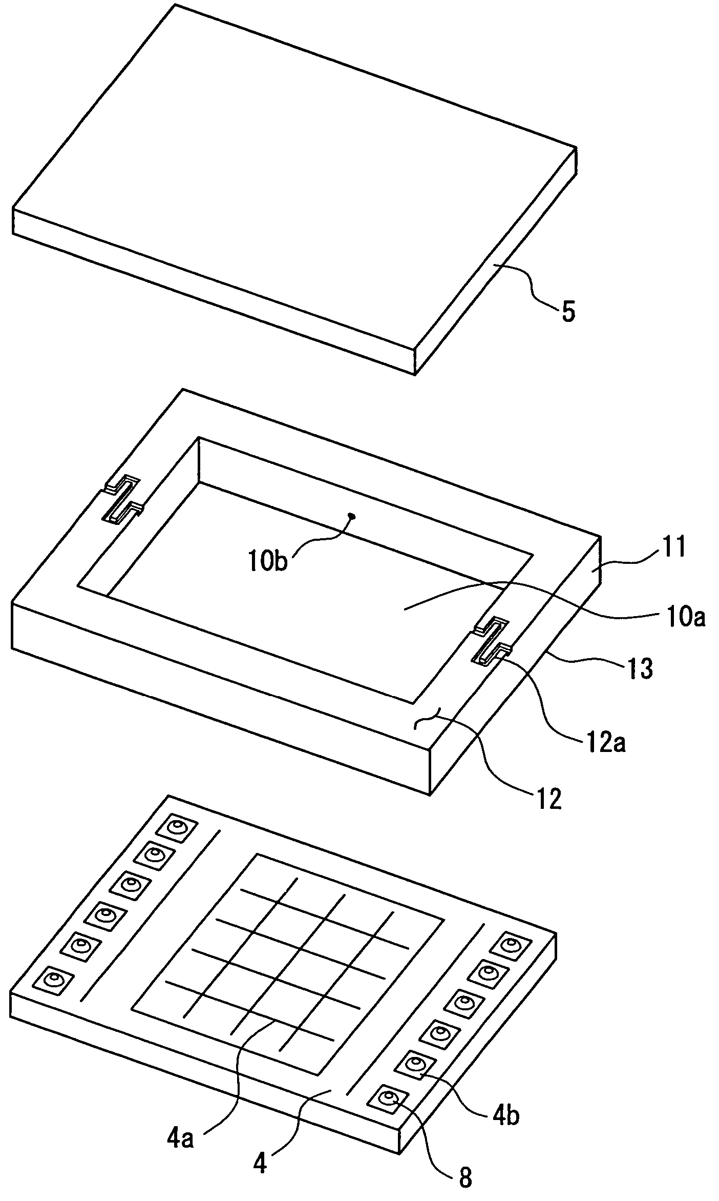
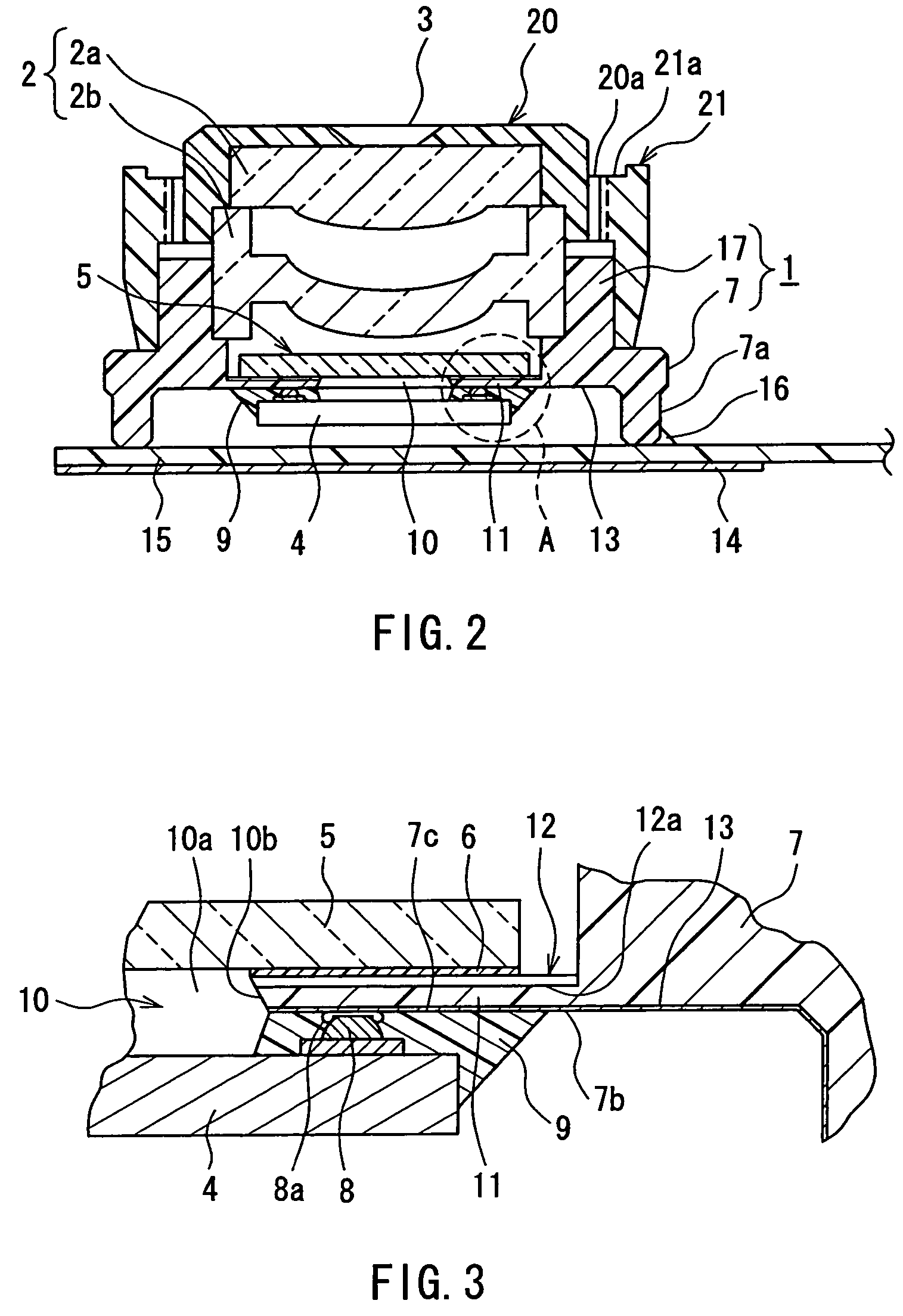
[0027]In the imaging apparatus according to the present invention, the opening of the three-dimensional substrate is enclosed with the optical filter and the semiconductor imaging device so as to form a cavity, and the air passage for allowing the cavity to communicate with the exterior has the labyrinth structure that causes a flow rate of air passing through the air passage to vary depending on a location in the air passage. Thus, for example, in a process of fabricating an imaging apparatus, the entry of foreign matter into a module can be prevented, thereby facilitating thickness reduction and improving workability in fabrication.

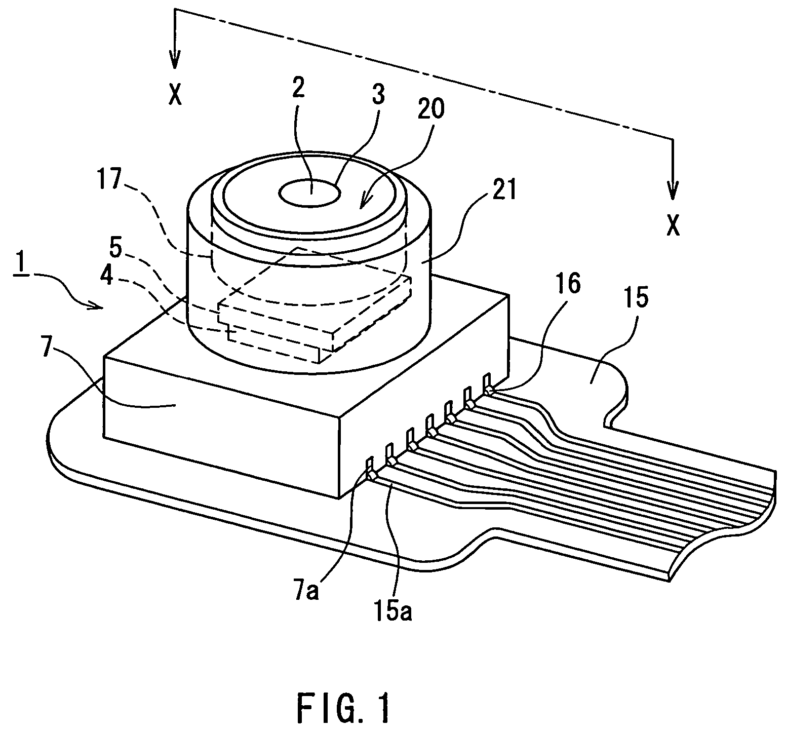
[0028]Hereinafter, the present invention will be described by way of an embodiment with reference to the appended drawings. Referring first to FIGS. 1 to 3, the description is directed to the configuration of an imaging apparatus according to this embodiment.

[0029]FIG. 1 is a perspective view of the imaging apparatus. A three-dimensional substrate 1 is ...


PUM


Abstract

An imaging apparatus includes: a three-dimensional substrate in which a partition wall (11) having an opening (10a) at a central portion is formed so as to cross an inner cavity; an optical filter (5) that is fixed on a first flat surface (12) of both surfaces of the partition wall so as to cover the opening; a semiconductor imaging device (4) that is face-down mounted on a second flat surface (13) of the partition wall with an imaging area (4a) facing the opening; and an optical system for forming images that is installed on a side of the optical filter in the inner cavity of the three-dimensional substrate. The opening of the partition wall is dosed on both sides with the optical filter and the semiconductor imaging device so as to form a cavity. An air passage (12a) for allowing communication between the cavity and an exterior of the three-dimensional substrate is formed on the first flat surface, and has a labyrinth structure that causes a flow rate of air passing through the air passage to vary depending on a location in the air passage. This allows air circulation between the exterior and a cavity enclosed by a semiconductor imaging device and an optical filter, while suppressing the entry of foreign matter from the exterior into the cavity via an airflow caused by expansion / contraction of air.

Description

TECHNICAL FIELD[0001]The present invention relates to an imaging apparatus using a semiconductor imaging device, which is reduced in size and thickness and used mainly in a camera mounted in portable equipment or the like, and a method for manufacturing the same.BACKGROUND ART[0002]Conventional imaging apparatuses of this kind have a structure described in JP2001-245186 A, for example. In the structure, a semiconductor imaging device configured of a CCD (Charge Coupled Device) or the like is mounted with a lens on a three-dimensional substrate and converts a focused image formed by the lens into an electric signal so that the image can be output.[0003]The three-dimensional substrate is composed of a base part having a rectangular planar shape and a cylindrical barrel part disposed on an upper portion of the base part, and an opening is formed on a boundary between the base part and the barrel part. The lens is fitted against an inner peripheral surface of the barrel part. With an op...

Claims


Application Information

Patent Timeline
Patent Type & Authority Patents(United States)
IPC IPC(8): G03D17/00H04N5/225H01L27/14H04N5/335
CPCH04N5/2254H04N23/52H04N23/57H04N23/55H04N23/00
Inventor NISHIZAWA, HIROSHI
Owner PANASONIC CORP
Why Eureka
Try Eureka