Substrate before insulation, method of manufacturing substrate, method of manufacturing surface acoustic wave transducer, surface acoustic wave device, and electronic equipment

a technology of substrate and insulating layer, which is applied in the direction of instrumentation, circuit masks, photomechanical equipment, etc., can solve the problems of insufficient resist thickness, insufficient manufacturing cost, and fluctuation of frequency and instability of resonance characteristics, so as to shorten the process of manufacturing substrate, easy to remove protection film, and simplify the effect of the instrument manufacturing substra

Inactive Publication Date: 2009-05-19
SEIKO EPSON CORP
View PDF9 Cites 2 Cited by
  • Summary
  • Abstract
  • Description
  • Claims
  • Application Information

AI Technical Summary

Benefits of technology

[0008]One of advantages of the invention is to provide a substrate before an insulation process, including a protection film having a sufficient strength (the strength of adhesiveness) against an insulation process. The other of advantages of the invention is to provide a method of manufacturing a substrate or a surface acoustic wave transducer, in which only a desired part can be treated with insulation among a conductive portion of a surface. Further, the other of advantages of the invention is to provide a highly reliable surface acoustic wave transducer, surface acoustic wave device, and electronic equipment.

Problems solved by technology

In such surface acoustic wave transducer, attaching a conductive foreign materials to the surface of an IDT causes a problem of fluctuation of frequency and instability of resonance characteristics.
Further, no mask is needed because of omitting a process for developing a resist, constraining a manufacturing cost.
However, if a resist is given by an inkjet method, the thickness of a resist is insufficient.
This insufficiency of the thickness of a resist at the circumferential area, in particular, causes an anodic oxidation liquid to leak in the interface between a conductive pad and a resist film from the circumference of a resist film during anodic oxidation process, forming an oxide film in a part of a region in which a resist film is placed.
Further, the insufficient thickness at the center of a resist film causes an insufficient strength against an anodic oxidation liquid at this part (the strength of adhesiveness), making a part of the center area of a resist film remove during a anodic oxidation process.
Thus, it is uneasy that a liquid for insulation process leaks into the interface between a surface of the base and the protection film, when the surface of the base is treated with insulation by dipping the base into a liquid for insulation process, for example.
Further, a part of the protection film can not removed when being treated with insulation.
According to this processes, it is uneasy that a liquid for insulation process leaks in the interface between a surface of the base and the protection film, when the surface of the base is treated with insulation by dipping the base into a liquid for insulation process, for example since the protection film includes the first protection layer having the circumferential partition wall.
Further, in the processes, the sufficient thickness is assured along with an entire protection film and a part of protection film can not be removed when being treated with insulation since the second protection layer is placed in a area surrounded by the circumferential partition wall.

Method used


Image

  • Substrate before insulation, method of manufacturing substrate, method of manufacturing surface acoustic wave transducer, surface acoustic wave device, and electronic equipment
  • Substrate before insulation, method of manufacturing substrate, method of manufacturing surface acoustic wave transducer, surface acoustic wave device, and electronic equipment
  • Substrate before insulation, method of manufacturing substrate, method of manufacturing surface acoustic wave transducer, surface acoustic wave device, and electronic equipment

Examples


modification 1

[0112

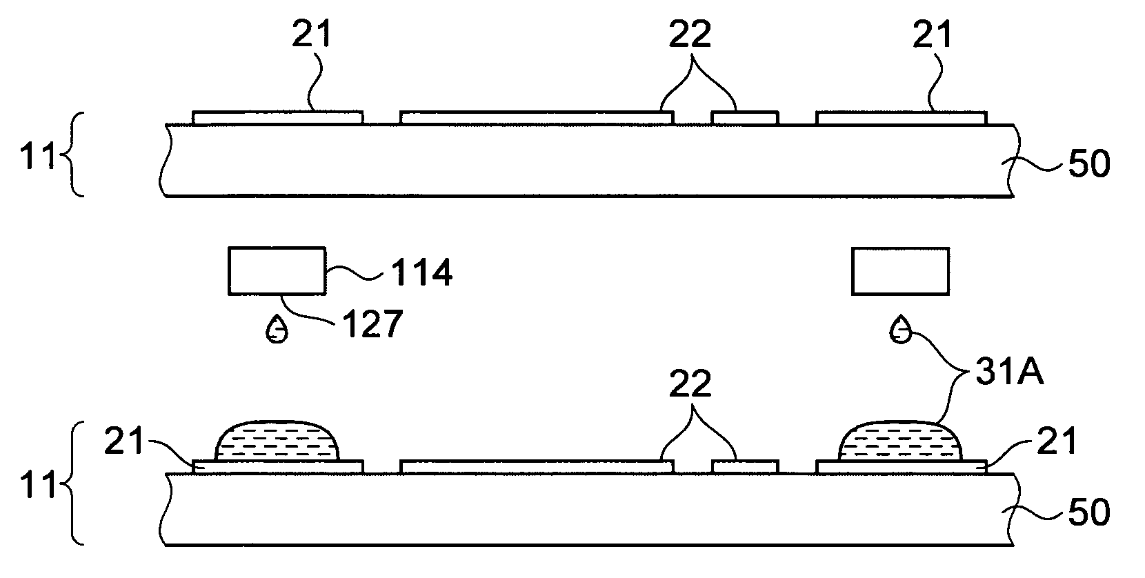
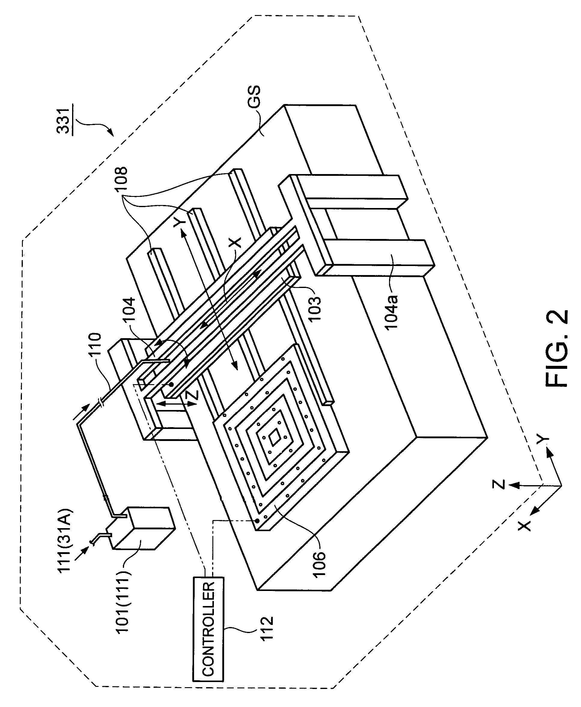
[0113]The above mentioned embodiment includes the process of heating the base 11 by the heater 320 for forming the protection layer 31 which is higher than the thickness of the partition wall 33 and the process of giving the first protection material 31A to the surface of the base 11 by using the droplet-discharging device 331. But, instead of these processes, the first protection material 31A in which the boiling temperature of the solvent is more than 170° C. and under 250° C. may be discharged to the surface of the base by using the droplet-discharging device 331. This is a modification where the ratio a / b can be increased by increasing the boiling temperature of the solvent in the first protection material 31A more than increasing the temperature of the base 11. According to the inventor's experiment, when the boiling temperature of the solvent in the first protection material 31A is more than 170° C. and under 250° C. without heating the base 11, the protection layer 30 ha...

modification 2

[0116

[0117]In the above embodiment, the first protection layer 31 included in the protection film 30 comprises the circumferential partition wall 33 and the ground film 34 which is integrally formed with the circumferential partition wall 33. But, the ground film 34 may be omitted. FIGS. 15A and 15B show this modification. In FIGS. 15A and 15B, the first protection layer 31 only comprises the circumferential partition wall 33, which is placed outer circumferential area of the protection region and the second protection layer 32 is placed so as to be embedded covering over the region surrounded by the partition wall. The protection film 30 comprises the first protection layer 31 and the second protection layer 32 and is placed on a surface of a part of the base 11. FIG. 15B is an enlarged view of the conductive pad 21 of the base 11 and FIG. 15A is a cross section when the base 11 is cut along the line E-E in FIG. 15B. Thus, in the protection film 30 including the first protection la...

modification 3

[0120

[0121]In the above mentioned embodiment, anode oxidization process was used for insulating the surface of the aluminum thin film, but any other methods may be used if a layer for insulating the surface of the base 11 can be formed. For example, the thermal oxidization may be used in which the base 11 is put into a processing unit filled with a gas such as oxygen and heated. Thus, the substrate having the insulation layer 40 only in the desired area among the surface of the base may be manufactured by this method for manufacturing the base including such insulation process.


PUM

PropertyMeasurementUnit
boiling pointaaaaaaaaaa
temperatureaaaaaaaaaa

Abstract

A substrate before an insulation process, which is provided with a protection film to prevent a part of a surface area, which has electrical conductivity from being insulated, the substrate comprises: a base including the surface area, which has electrical conductivity; a protection film covering over the part of the surface area, which has electrical conductivity, and being formed on the base; the protection film including; a first protection layer having a circumferential partition wall and a second protection layer placed and embedded in an area, which is surrounded by the circumferential partition wall.

Description

BACKGROUND[0001]1. Technical Field[0002]The present invention relates to a substrate before an insulation process, which is provided with a protection film to prevent a part of an surface area, which has electrical conductivity, from being treated with insulation, a method of manufacturing a substrate with being insulated, a method of manufacturing a surface acoustic wave transducer, a surface acoustic wave transducer manufactured by this method, a surface acoustic wave device, and electronic equipment.[0003]2. Related Arts[0004]A surface acoustic wave transducer for electrically driving surface acoustic wave (SAW) or detecting it is manufactured by forming an interdigital transducer (IDT), a reflector and a conductive pad made of an aluminum thin film on the surface of a piezoelectric substance such as a quartz. In such surface acoustic wave transducer, attaching a conductive foreign materials to the surface of an IDT causes a problem of fluctuation of frequency and instability of ...

Claims


Application Information

Patent Timeline
Patent Type & Authority Patents(United States)
IPC IPC(8): C25D5/02
CPCH03H3/08H03H9/0542H05K3/0079B81B2201/0271H05K3/02H05K2203/013H05K2203/0315H05K2203/0577H05K2203/1142H05K2203/1476G10D7/04G10D9/00
Inventor HASEI, HIRONORI
Owner SEIKO EPSON CORP
Why Eureka
Try Eureka