Structure of substrate

a substrate and structure technology, applied in the field of substrates, can solve the problems of affecting the performance and life of the heat source b>120/b>, stabilizing the operation of the heat source, etc., and achieves the effects of reducing the resistivity of the transmission pathway, high heat dissipation capacity, and high electrical transmission performan

Active Publication Date: 2009-05-19
UNIMICRON TECH CORP
View PDF4 Cites 2 Cited by
  • Summary
  • Abstract
  • Description
  • Claims
  • Application Information

AI Technical Summary

Benefits of technology

[0014]According to the aforementioned techniques, the present invention includes at least the following advantages. Firstly, because the conductive pathways between the top surface and the bottom surface of the substrate do not include any high thermal resistant insulating layer but include only through two mutually connected patterned metallic layers in the metallic panel, the substrate has a high heat-dissipating capacity. Secondly, because a portion of the patterned metallic layers is directly connected with each other and the cross-sectional area of the metallic circuit perpendicular to the current flowing direction is rather large, the resistivity of the transmission pathways can be reduced. Hence, a higher electrical transmission performance can be attained.

Problems solved by technology

However, with the miniaturization of products, an efficient method of dissipating heat away from a high-power chip such as a power chip or a light-emitting diode and hence stabilizing its operation has become a dominant issue in the design of electronic products.
Because the heat-dissipating pathways can hardly provide the heat-dissipating rate demanded by the heat source 120, the performance and life of the heat source 120 will be adversely affected.

Method used


Image

  • Structure of substrate
  • Structure of substrate
  • Structure of substrate

Examples


first embodiment

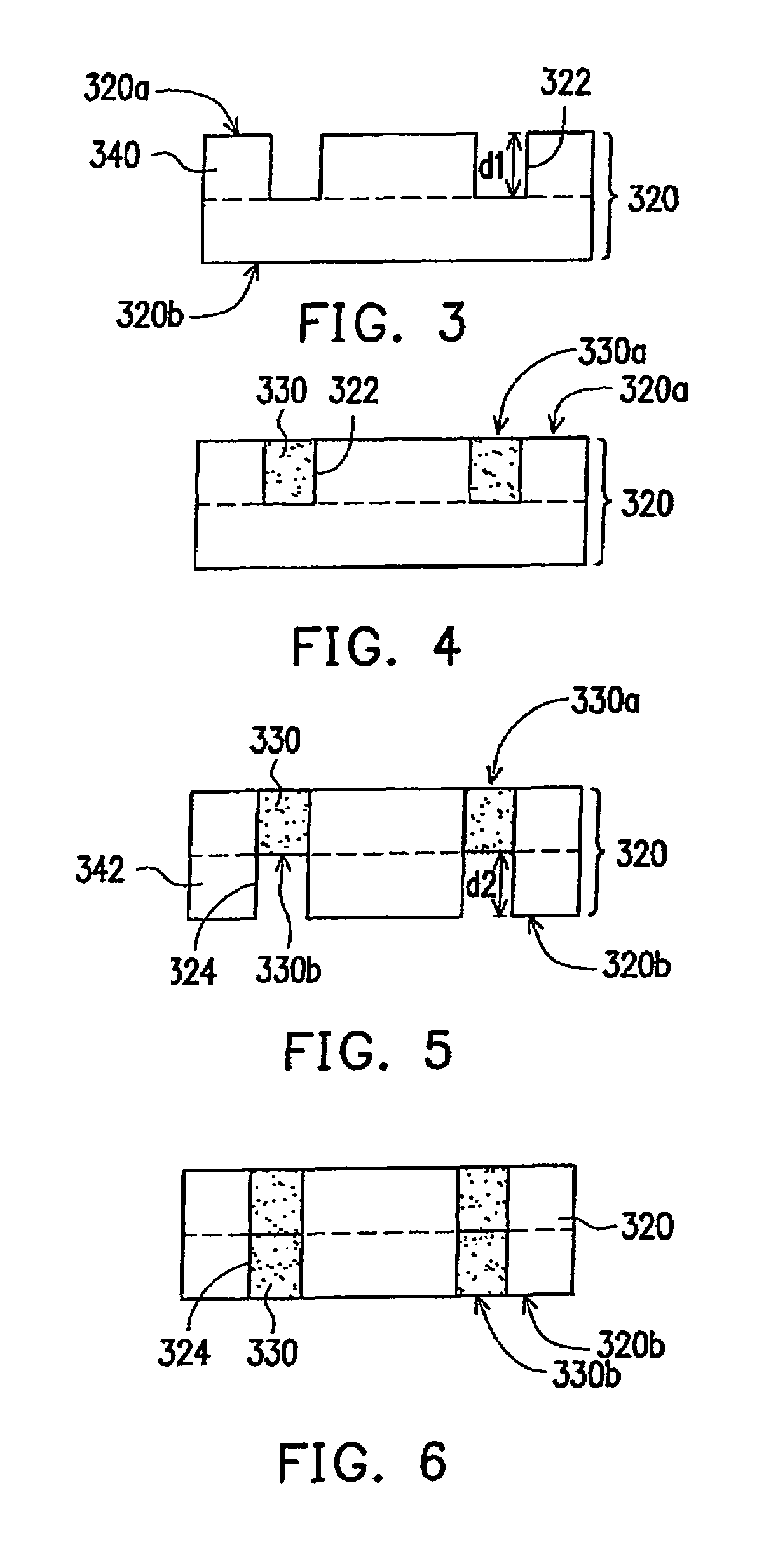
[0030]FIGS. 3 through 7 are schematic cross-sectional views showing the process of fabricating a substrate according to the present invention. As shown in FIG. 3, a metal panel 320 having a top surface 320a and a bottom surface 320b is provided. Then, a first half-etching process is performed to etch the top surface 320a of the metallic panel 320 to a first depth d1 and form a patterned metallic layer 340 on the top surface 320a. The first half-etching process includes the following steps. First, a photoresist layer (not shown) is formed on the top surface 320a and the bottom surface 320b. Thereafter, a photo-exposure and development process of the photoresist layer on the top surface 320a is carried out to pattern the photoresist layer and expose a portion of the top surface 320a. Using the photoresist layer as a mask, the exposed metallic panel 320 on the top surface 320a is etched to a first depth d1 to form a patterned metallic layer 340 such that gaps 322 are formed between the...

second embodiment

[0037]FIGS. 8 through 10 are schematic cross-sectional views showing the process of fabricating a substrate according to the present invention. FIGS. 8A, 9A and 10A are the top views of FIGS. 8, 9 and 10 in the process of fabricating a substrate. In fact, FIG. 8 is a cross-sectional view along line I-I of FIG. 8A, FIG. 9 is a cross-sectional view along line II-II of FIG. 9A and FIG. 10 is a cross-sectional view along line III-III of FIG. 10A.

[0038]As shown in FIGS. 8 and 8A, a metallic panel 420 is provided. Then, a mechanical punch process, for example, is used to punch a plurality of vias 422 passing through the metallic panel 420.

[0039]As shown in FIGS. 9 and 9A, polymer is deposited into the vias 422 and then cured by heating to form insulators 430. Thereafter, a polishing operation is carried out to polish the top surface 420a of the metallic panel 420 and remove any protruding insulators 430 outside the vias 422 so that the top surface 430a of the insulators 430 are coplanar w...


PUM

PropertyMeasurementUnit
thicknessaaaaaaaaaa
total thicknessaaaaaaaaaa

Abstract

A substrate having a metallic panel and an insulator is provided. The metallic panel comprises two patterned metallic layers. The two patterned metallic layers are disposed on the respective sides of the metallic panel and connected with each other. The metallic panel has an upper surface and a lower surface. The heat dissipating pathway between the upper and the lower surface is constructed using a metal. The insulator is positioned in the gaps between the patterned metallic layers.

Description

CROSS-REFERENCE TO RELATED APPLICATION[0001]This application claims the priority benefit of Taiwan application serial no. 94100031, filed on Jan. 3, 2005. All disclosure of the Taiwan application is incorporated herein by reference.BACKGROUND OF THE INVENTION[0002]1. Field of the Invention[0003]The present invention relates to a substrate and a method of fabricating the same. More particularly, the present invention relates to a substrate having an improved thermal and electrical conductivity and a method of fabricating the same.[0004]2. Description of the Related Art[0005]The roles played by information products in this highly commercialized society is increasingly important. With the rapid development of information products, most electronic products have multiple functions and an increasingly miniaturized and streamlined body. Furthermore, the quality of the product is also increasingly stable. However, with the miniaturization of products, an efficient method of dissipating heat...

Claims


Application Information

Patent Timeline
Patent Type & Authority Patents(United States)
IPC IPC(8): H01L23/10H01L35/34H05K5/00
CPCH01L23/142H05K3/06H05K3/202H01L21/6835H01L33/486H01L33/62H01L33/642H05K2201/09881H05K2203/0369H05K2203/1476H01L2224/32245H01L2224/48091H01L2224/48247H01L2224/73265H01L2924/00012H01L2924/00H01L2924/181H01L2924/00014
Inventor TSENG, TZYY-JANGCHANG, CHIH MINGYU, CHENG POHO, CHUNG W.
Owner UNIMICRON TECH CORP
Why Eureka
Try Eureka