Distributed electronic design automation environment

a technology of electronic design and automation environment, applied in the direction of instruments, cad networks, cad techniques, etc., can solve the problems of difficult or impossible representation of parts on a single sheet of a schematic diagram, the difficulty of electronic design approach, and the loss of schematic valu

Active Publication Date: 2009-06-09
SIEMENS PROD LIFECYCLE MANAGEMENT SOFTWARE INC
View PDF115 Cites 123 Cited by
  • Summary
  • Abstract
  • Description
  • Claims
  • Application Information

AI Technical Summary

Problems solved by technology

This traditional approach to electronic design presents numerous problems.
As designs have evolved, however, the schematic diagram has become less valuable.
Such parts can be difficult or impossible represent on a single sheet of a schematic diagram.
Drawing pieces of the same part on multiple drawing sheets can be tedious, and the resulting diagram is often confusing.
Similarly, modern designs often have complex patterns of interconnections which run throughout the entire design, and must thus span numerous sheets of schematic diagrams.
Following such interconnection patterns across multiple sheets is also tedious and confusing.
However, the complexity of electronic designs and market pressures to rapidly complete designs are continuing to increase.
Traditional methods can also inhibit collaboration among multiple front-end designers.
Separating a design project into manageably-sized portions and assigning those portions to different designers can be difficult.
Moreover, managing design data as a collection of design data computer files limits the granularity with which design data can be “locked” to prevent conflicting edits by multiple users.
File-based systems pose additional challenges for designers wishing to collaborate on a project.
For example, a designer may often be unsure whether he or she has all of the files needed for a particular project.
This also makes transfer of a design between designers a time-consuming process.
Traditional electronic design methods are increasingly less valuable in other ways.
In addition to often having more LSI and VLSI parts, modern designs are becoming increasingly dense.
These factors make constraints upon the physical design more and more critical.
However, existing methods for constraint management become less useful as designs become more complex.
Constraint data must often be synchronized among multiple users in real time, and waiting for an updated schematic (with revised constraint annotations) or a separate constraint document can require too much time.
More important, lack of an automated system for synchronizing constraint data may result in a failure to effectively communicate constraint data between front and back ends.
Traditional design methods present other challenges for numerous persons working in parallel, particularly when those persons are in widely dispersed locations.
Ensuring that all of these groups have the appropriate software needed to edit or view design data can impose significant administrative burdens.
Yet a further complication arises when trying to limit the type of information accessible by certain groups.

Method used


Image

  • Distributed electronic design automation environment
  • Distributed electronic design automation environment
  • Distributed electronic design automation environment

Examples


Embodiment Construction

[0052]Connectivity-Centric Data Model

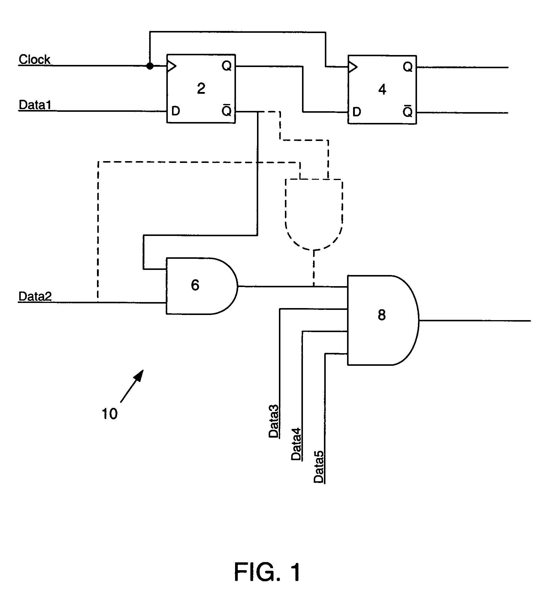
[0053]In many parts of the design process (in both the front and back ends), connectivity between circuit elements is more critical than a particular graphical representation of the circuit. FIG. 1, a schematic diagram for a portion of a hypothetical circuit 10, illustrates this point. Included in FIG. 1 are two flip-flops 2 and 4, an AND gate 6 and a four-way AND gate 8. Also shown in FIG. 1 are interconnections between inputs and outputs of these circuit elements, as well as connections to various signal lines (e.g., “Clock,”“Data1,” etc.) connected to other circuit elements not shown in FIG. 1. Although a schematic such as FIG. 1 may assist in visualizing signal flows and in understanding other aspects of a circuit design, the specific graphical form and arrangement of circuit element symbols is generally not critical to a front end designer. For example, the logical functionality of the circuit in FIG. 1 is unaffected if AND gate 6 is reorien...


PUM


Abstract

PCB Logical design data is stored in a database according to a connectivity-based data model. Circuit functional blocks, inputs and outputs of functional blocks, and signals are stored as separate data structures. Those structures may be edited by users at separate clients during concurrent editing sessions. Profile data for each of multiple users specifies logical design data elements accessible by, and PCB design software to be provided to, that user. The PCB design software may be plug-ins executable within a web browser at a client, and the client computers may communicate with the database via the Internet. Layout data may also be stored in the database, with elements of the layout data mapped to elements of the logical design data. Constraint data may also be stored in the database, with elements of the constraint data being mapped to elements of the layout data.

Description

COPYRIGHT NOTICE[0001]A portion of the disclosure of this patent document may contain material which is subject to copyright protection. To the extent that it does, the copyright owner has no objection to the facsimile reproduction by anyone of the patent document or the patent disclosure as it appears in the Patent and Trademark Office patent file or records, but otherwise reserves all copyright rights whatsoever. The following notice applies to the software and data as described below and in the drawings hereto: Copyright © 2004, Mentor Graphics Corp., All Rights Reserved.FIELD OF THE INVENTION[0002]This invention relates to the field of electronic design automation tools, and more specifically, to concurrent design activities distributed among multiple users.BACKGROUND OF THE INVENTION[0003]As used throughout this specification and claims, a “design” for an electronic device generally refers to information needed to construct that device. As can be appreciated from this broad def...

Claims


Application Information

Patent Timeline
Patent Type & Authority Patents(United States)
IPC IPC(8): G06F17/50G06F19/00G06F3/00
CPCG06F17/5045G06F2217/04G06F30/30G06F2111/02
Inventor MANKIN, RICHARDPOTTS, HENRYTERA, REDDY
Owner SIEMENS PROD LIFECYCLE MANAGEMENT SOFTWARE INC
Why Eureka
Try Eureka