Tuning programmable logic devices for low-power design implementation

a programmable logic and design implementation technology, applied in the direction of power consumption reduction, pulse technique, instruments, etc., can solve the problems of significantly higher static significantly higher dynamic power consumption of programmable logic devices, and unused resources still consuming static power, so as to achieve the effect of reducing power consumption

Active Publication Date: 2009-06-16
XILINX INC
View PDF58 Cites 19 Cited by
  • Summary
  • Abstract
  • Description
  • Claims
  • Application Information

AI Technical Summary

Benefits of technology

[0007]In accordance with one embodiment of the present invention, unused and / or inactive resources in a PLD are disabled to achieve lower power consumption.

Problems solved by technology

Programmable logic devices (PLDs), such as field programmable gate arrays (FPGAs), have a significantly higher static power consumption than dedicated logic devices, such as standard-cell application specific integrated circuits (ASICs).
However, these unused resources still consume static power in the form of leakage current.
Programmable logic devices (PLDs) also have a significantly higher dynamic power consumption than dedicated logic devices because the PLD resources (logic and routing) are designed with a fixed level of performance, regardless of the requirements of the specific application being implemented by the PLD.
In circuit design, higher speed circuits generally consume more power, both dynamic and static.
Consequently, the parts of the PLD that are not operated at the maximum hardware speed represent an inefficient use of power.
For example, if certain resources of the operating PLD are inactive for a predetermined time period, then the user-controlled signals may be activated, thereby causing the inactive resources to be disabled.
In addition, the active blocks in the second set meet the timing requirements of the PLD design, in spite of operating in response to the reduced VDD supply voltage, because of the large timing slack initially present in these blocks.

Method used


Image

  • Tuning programmable logic devices for low-power design implementation
  • Tuning programmable logic devices for low-power design implementation
  • Tuning programmable logic devices for low-power design implementation

Examples


Embodiment Construction

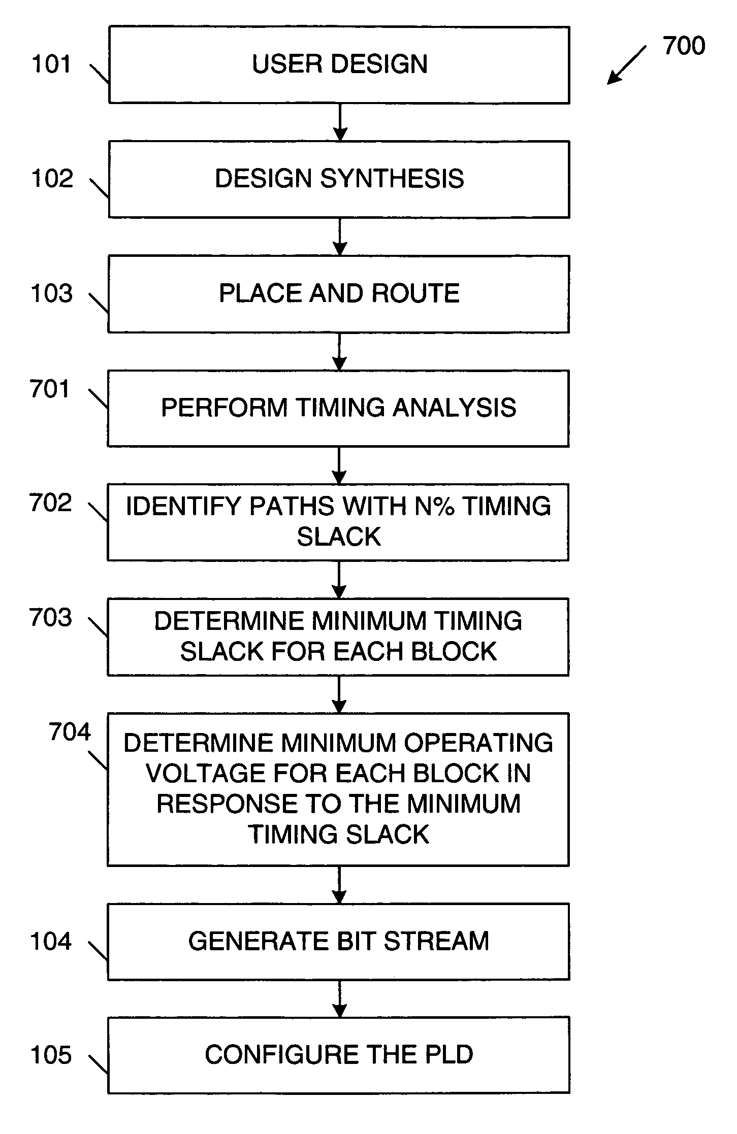
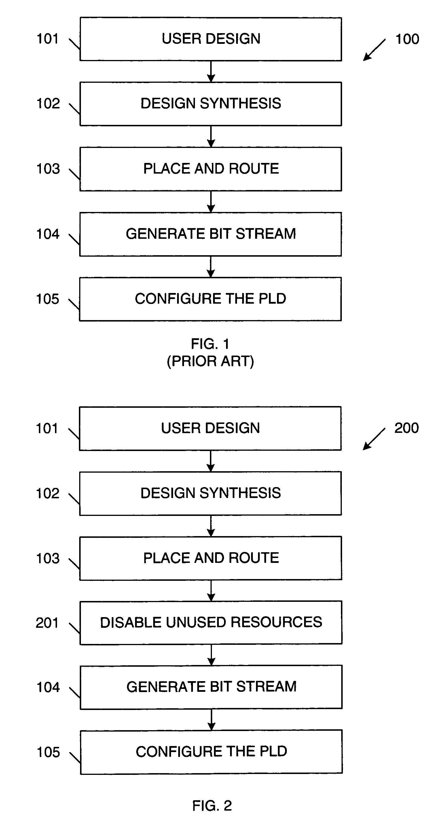
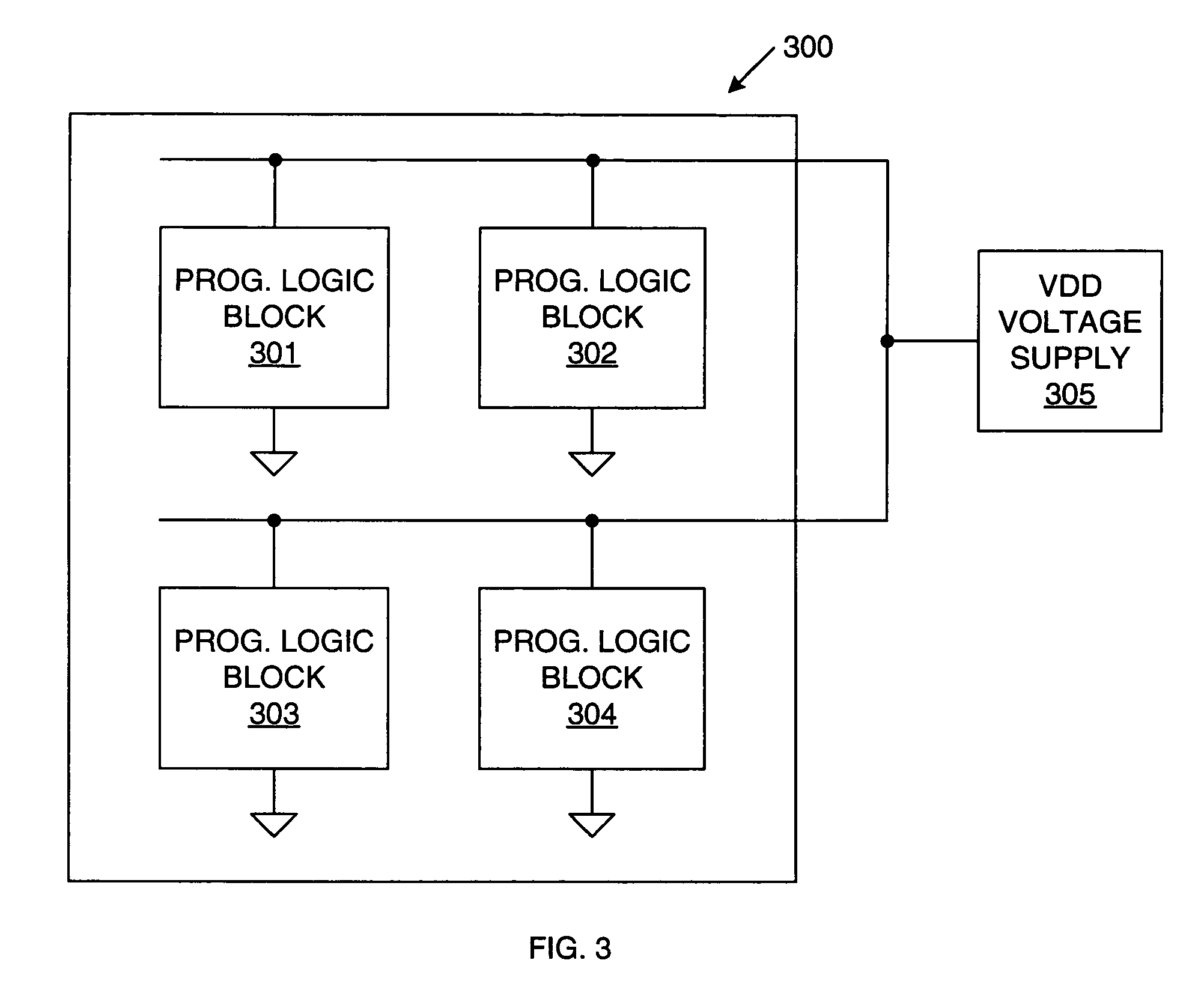
[0028]In accordance with one embodiment of the present invention, unused and inactive resources in a programmable logic device (PLD), such as a field programmable gate array (FPGA), are disabled to achieve lower static power consumption. The present invention includes both an enabling software flow and an enabling hardware architecture, which are described in more detail below. Unused resources of the PLD can be disabled when designing a particular circuit to be implemented by the PLD (hereinafter referred to as “design time”). In addition, resources of the PLD that are temporarily inactive can be disabled during operation of the PLD (hereinafter referred to as “run time”).

[0029]FIG. 1 is a flow diagram 100 illustrating a conventional design flow used for PLDs. Initially, a user designs a circuit to be implemented by the PLD (Step 101). This user design is described in a high-level specification, such as Verilog or VHDL. The high-level specification is first synthesized to basic log...


PUM


Abstract

A method of operating a programmable logic device includes the steps of using a full VDD supply voltage to operate a first set of active blocks of the programmable logic device, and using a reduced supply voltage (e.g., 0.9 VDD) to operate a second set of active blocks of the programmable logic device. A timing analysis is performed to determine the maximum available timing slack in each active block. Active blocks having a smaller timing slack are grouped in the first set, and are coupled to receive the full VDD supply voltage. Active blocks having a larger timing slack are grouped in the second set, and are coupled to receive the reduced VDD supply voltage. As a result, the active blocks in the second set exhibit reduced power consumption, without adversely affecting the overall speed of the programmable logic device.

Description

RELATED APPLICATION[0001]The present application is a continuation-in-part of U.S. patent application Ser. No. 10 / 666,669 filed by Tim Tuan, Kameswara K. Rao and Robert O. Conn on Sep. 19, 2003 now U.S. Pat. No. 7,098,689, which is incorporated herein in its entirety.FIELD OF THE INVENTION[0002]The present invention relates to the regulation of the supply voltage provided to unused and / or inactive blocks in a programmable logic device to achieve lower power consumption. More specifically, the present invention relates to selectively reducing the operating voltage of various sections of an integrated circuit device in order to reduce the leakage current and / or increase the performance of the device.RELATED ART[0003]Programmable logic devices (PLDs), such as field programmable gate arrays (FPGAs), have a significantly higher static power consumption than dedicated logic devices, such as standard-cell application specific integrated circuits (ASICs). A reason for this high static power...

Claims


Application Information

Patent Timeline
Patent Type & Authority Patents(United States)
IPC IPC(8): G06F17/50H03K19/00
CPCG11C5/14H03K19/0016H03K19/17784H03K19/17792H03K3/356173
Inventor TUAN, TIMDEJONG, JAN L.RAO, KAMESWARA K.CONN, ROBERT O.
Owner XILINX INC
Why Eureka
Try Eureka