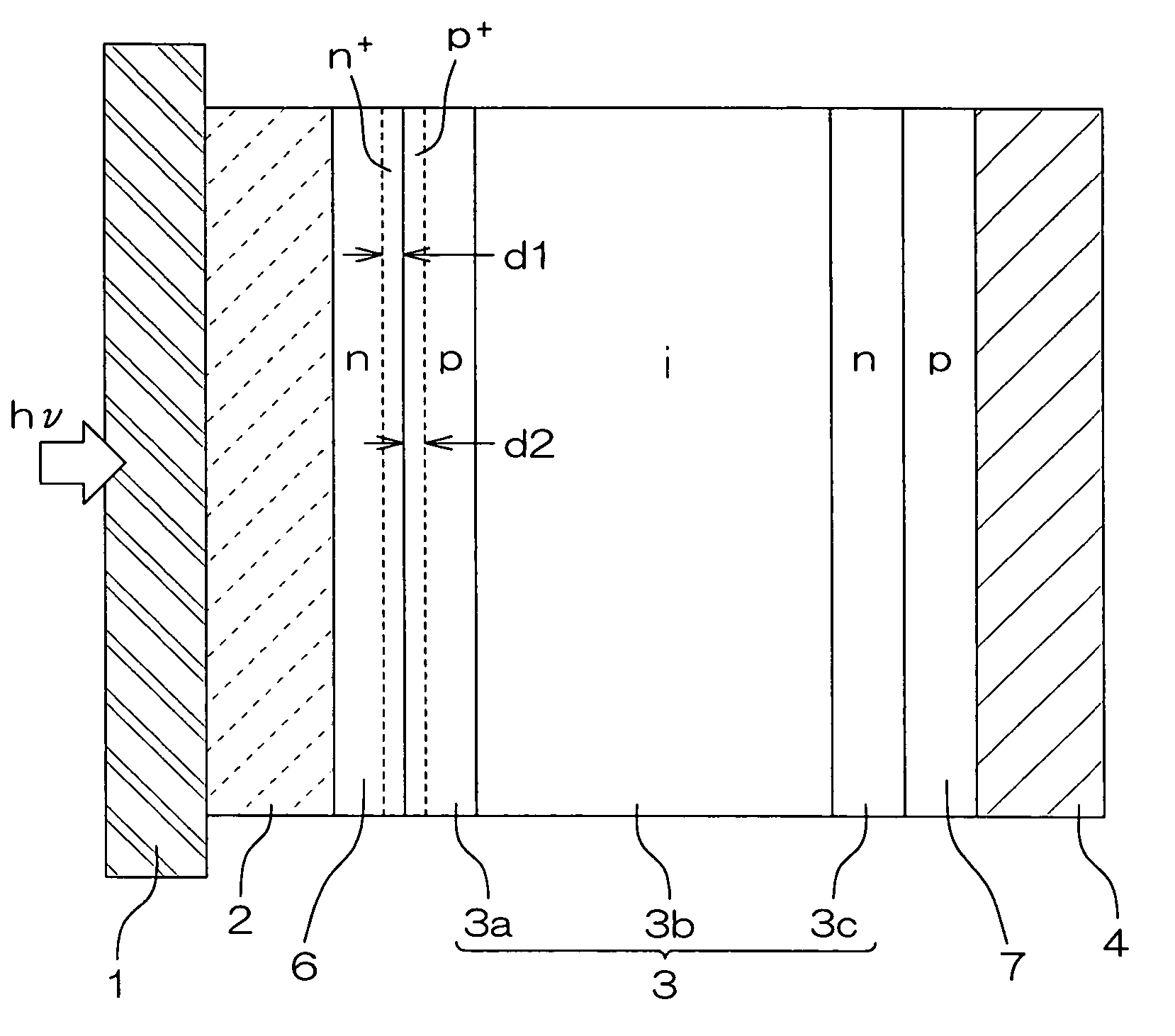
Solar cell device

a solar cell and contact structure technology, applied in the direction of superconductor devices, semiconductor devices, electrical devices, etc., can solve the problem of limitation of obtained effect, and achieve the effect of reducing the carrier recombination rate r and reducing the recombination center density nr

Inactive Publication Date: 2009-07-14
KYOCERA CORP
View PDF23 Cites 31 Cited by
  • Summary
  • Abstract
  • Description
  • Claims
  • Application Information

AI Technical Summary

Benefits of technology

[0037]As a result of examination, the inventors have found a configuration which allows a recombination center density Nr to be reduced without increasing a minority carrier density n and consequently, allows a carrier recombination rate R in a semiconductor / electrode contact interface to be effectively reduced.
[0089]Particularly in the photoelectric conversion device, the recombination rate of the photo-generated carriers excited by incident light can be effectively reduced, and the dark current component can be effectively prevented from being produced, thereby allowing photoelectric conversion efficiency to be improved. The carrier recombination rate is significantly reduced in excess of a certain threshold value, so that obtained characteristics are significantly stabilized, thereby making it possible to obtain the effect of significantly improving the yield of the semiconductor device.

Problems solved by technology

However, there are some problems.
Therefore, an obtained effect has a limitation.

Method used


Image

  • Solar cell device
  • Solar cell device
  • Solar cell device

Examples


example 1

[0301]The thin film silicon solar cell device was manufactured on the basis of the configuration shown in FIG. 3 in the present invention. Manufacturing conditions are shown in Table 1.

[0302]

TABLE 1p-typesemiconductorFirstn-type semiconductor layer 31dlayer 31aelectrode 2Doping elementElement forBand gapSi crystalDoping elementSampleConstituentconcentrationThicknessenlargingwidthphase isconcentrationNo.material(cm−3)(nm)band gap(eV)included(cm−3)*1SnO2—————1E19~7E202SnO23E19~1E212—1.1~1.3◯1E19~7E203SnO2—————1E19~7E204SnO23E19~1E212—1.1~1.3◯1E19~7E20*5SnO25E+172—1.1~1.3◯1E19~7E206SnO22E+182—1.1~1.3◯1E19~7E207SnO23E+212—1.1~1.3◯1E19~7E20*8SnO26E+212—1.1~1.3◯1E19~7E209SnO23E19~1E214—1.1~1.3◯1E19~7E2010SnO23E19~1E217—1.1~1.3◯1E19~7E2011SnO23E19~1E2118 —1.1~1.3◯1E19~7E2012SnO23E19~1E2125 —1.1~1.3◯1E19~7E20*13SnO23E19~1E212—1.1~1.3◯1E19~7E2014SnO23E19~1E212—1.1~1.3◯1E19~7E2015SnO23E19~1E212—1.1~1.3◯1E19~7E20*16SnO23E19~1E212—1.1~1.3◯1E19~7E2017SnO23E19~1E212—1.1~1.3◯1E19~7E2018SnO23E19~1E...

example 2

[0316]The bulk type solar cell device shown in FIG. 6 according to the present invention was manufactured in the following manner. Manufacturing conditions are shown in Table 3.

[0317]

TABLE 3Frontp-type Si-BSFRearelectrodep-type Si region 503n-type Siregion 506n-type Si region 507electrode501Dopingregion 504DopingDoping508MainelementThick-Si crystalDoping elementelementelementThick-Si crystalMainSampleconstituentconcentrationnessphase isconcentrationconcentrationconcentrationnessphase isconstituentNo.material(cm−3)(nm)included(cm−3)(cm−3)(cm−3)(nm)includedmaterial*1Ag——◯2E19~2E212E18~1E19——◯Ag2Ag1E+195◯2E19~2E212E18~1E19——◯Ag3Ag——◯2E19~2E212E18~1E193E+1910◯Ag4Ag1E+195◯2E19~2E212E18~1E193E+1910◯Ag* is an example outside the scope of the present invention.

[0318]A p-type Si substrate having a thickness of 300 μm (a dopant B concentration is 2×1016 cm−3) was taken as the p-type Si photoactive region 505, and the n-type Si region 504 was formed thereon so that the doping element concentra...

example 3

[0327]The thin film silicon solar cell device having the configuration shown in FIG. 7 according to the present invention was manufactured. Manufacturing conditions are shown in Table 5.

[0328]

TABLE 5Trans-p-typen-typeparentlayerlayer 31cp-type layer 31dinter-n-type layer 32d32aDopingDopingElementSimediateDopingElementSiDopingelementelementfor en-Bandcrystallayer 5elementfor en-BandcrystalelementSam-concen-concen-Thick-larginggapphaseCon-concen-Thick-larginggapphaseconcen-pletrationtrationnessbandwidthis in-stituent trationnessbandwidthis in-trationNo.(cm−3)(cm−3)(nm)gap(eV)cludedmaterial(cm−3)(nm)gap(eV)cluded(cm−3)*13E19~1E21—————ZnO————01E19~7E2023E19~1E213E19~1E212—1.1~1.3◯ZnO—————1E19~7E2033E19~1E21—————ZnO1E19~7E205—1.1~1.3◯1E19~7E2043E19~1E213E19~1E212—1.1~1.3◯ZnO1E19~7E205—1.1~1.3◯1E19~7E2053E19~1E215E172—1.1~1.3◯ZnO1E19~7E205—1.1~1.3◯1E19~7E2063E19~1E212E182—1.1~1.3◯ZnO1E19~7E205—1.1~1.3◯1E19~7E2073E19~1E213E212—1.1~1.3◯ZnO1E19~7E205—1.1~1.3◯1E19~7E2083E19~1E216E212—1.1~1.3◯...


PUM


Abstract

In a photoelectric conversion device, in a contact between a p-type semiconductor 3a and an electrode 2, an n-type semiconductor 6 of a conductivity type opposite to that of the p-type semiconductor is provided between the p-type semiconductor 3a and the electrode 2. The existence of the n-type semiconductor 6 allows a recombination rate of photo-generated carriers excited by incident light to be effectively reduced, and allows a dark current component to be effectively prevented from being produced. Therefore, it is possible to improve photoelectric conversion efficiency as well as to stabilize characteristics. Further, a tunnel junction is realized by increasing the concentration of a doping element in at least one or preferably both of the p-type semiconductor 3a and the n-type semiconductor 6 in a region where they are in contact with each other, thereby keeping ohmic characteristics between the semiconductor and the electrode good.

Description

[0001]This application is based on application Nos. 2003-182584 and 2003-201417 filed in Japan, the content of which is incorporated hereinto by reference.BACKGROUND OF THE INVENTION[0002]1. Field of the Invention[0003]The present invention relates to a semiconductor / electrode contact structure, and a semiconductor device using the same. Examples of the semiconductor device include a photoelectric conversion device such as a solar cell device, a diode, a transistor, and a thyristor.[0004]2. Description of the Related Art[0005]A semiconductor device has a contact between an electrode composed of a metal or a conductive material such as a conductive oxide material and a semiconductor. On the side of the semiconductor in the semiconductor / electrode contact, a defect level called an interface level is generally produced. Such a defect level occurs due to impurities and distortion, non-equilibrium in a semiconductor forming process, etc., and functions as a carrier recombination center. ...

Claims


Application Information

Patent Timeline
Patent Type & Authority Patents(United States)
IPC IPC(8): H01L29/74H01L29/06H01L29/43H01L31/0224H01L31/042H01L31/076H01L31/105
CPCH01L31/022408H01L31/022425H01L31/1055H01L31/076Y02E10/548Y02E10/52
Inventor NIIRA, KOICHIROSENTA, HIROFUMIHAKUMA, HIDEKI
Owner KYOCERA CORP
Why Eureka
Try Eureka