Fluorescent material having two layer structure and light emitting apparatus employing the same

a fluorescent material and light-emitting apparatus technology, applied in the direction of discharge tube luminescnet screens, semiconductor lasers, sustainable buildings, etc., can solve the problems of reducing the emission intensities of blue and green fluorescent materials constituting white light, and the emission efficiency of the emission apparatus is not sufficient for serving as an illuminator, so as to achieve excellent emission efficiency and excellent color rendering

Inactive Publication Date: 2009-07-14
FUJITA SHIZUO +4
View PDF25 Cites 60 Cited by
  • Summary
  • Abstract
  • Description
  • Claims
  • Application Information

AI Technical Summary

Benefits of technology

[0007]In consideration of the aforementioned problem, an object of the present invention is to provide a fluorescent material excellent in emission efficiency for white emission and a light-emitting apparatus excellent in color rendering employing the same.
[0010]The first fluorescent material according to the present invention causes no light absorption when employed along with blue and green illuminants, and does not damage green and blue emission intensities in white emission resulting from color mixing. Therefore, white emission excellent in color purity and color rendering can be obtained.
[0012]The second fluorescent material according to the present invention causes no light absorption when employed along with a blue illuminant, and does not damage the blue emission intensity in white emission resulting from color mixing. Therefore, white emission excellent in color purity and color rendering can be obtained.
[0021]The light-emitting apparatus according to the present invention causes no light absorption when employing the aforementioned-first and second fluorescent materials with a blue illuminant, and does not damage green and blue emission intensities in white emission. Therefore, the light-emitting apparatus can present white emission excellent in color purity and color rendering.

Problems solved by technology

When the inventors prepared a white light-emitting apparatus according to the technique described in the aforementioned Japanese Patent Laying-Open No. 11-340516, however, it was recognized that the emission intensities of blue and green fluorescent materials constituting white light were remarkably reduced as compared with a red fluorescent material to damage the color balance and the light-emitting apparatus attained neither sufficient color rendering nor sufficient emission efficiency for serving as an illuminator.

Method used


Image

  • Fluorescent material having two layer structure and light emitting apparatus employing the same
  • Fluorescent material having two layer structure and light emitting apparatus employing the same
  • Fluorescent material having two layer structure and light emitting apparatus employing the same

Examples


example 1

[0101]According to Example 1, the present invention was applied to a red fluorescent material employing group III nitride semiconductors.

[0102]A fluorescent material comprising a two-layer structure of a core of InN having a particle size of 13 nm and a shell of In0.1Ga0.9N covering this core was prepared (such a fluorescent material comprising a core and a shell both made of InxGa1−xN (0 ≦x≦1) is hereinafter referred to as “InGaN fluorescent material”). According to Example 1, the InGaN fluorescent material was deposited on a sapphire substrate by laser ablation. More specifically, targets of sintered bodies of InN and In0.1Ga0.9N were alternately ablated with a KrF excimer laser and the optical output of the laser and the ablation timing were so controlled that the core was coated with the InGaN target for forming the shell before the InN target for forming the core was scattered at a desired particle size and reached the sapphire substrate. When the emission spectrum of the InGaN...

example 2

[0106]According to Example 2, 3-mercaptopropyl trimethoxysilane and sodium citrate were added to a fluorescent material comprising a two-layer structure of a core of InN having a particle size of 14 nm and a shell of In0.1Ga0.9N having a particle size of 3 μm covering this core for adsorbing SiO2 molecules to the surface of the shell by surface reaction. Also according to Example 2, the InGaN fluorescent material was deposited on a sapphire substrate by laser ablation similarly to Example 1.

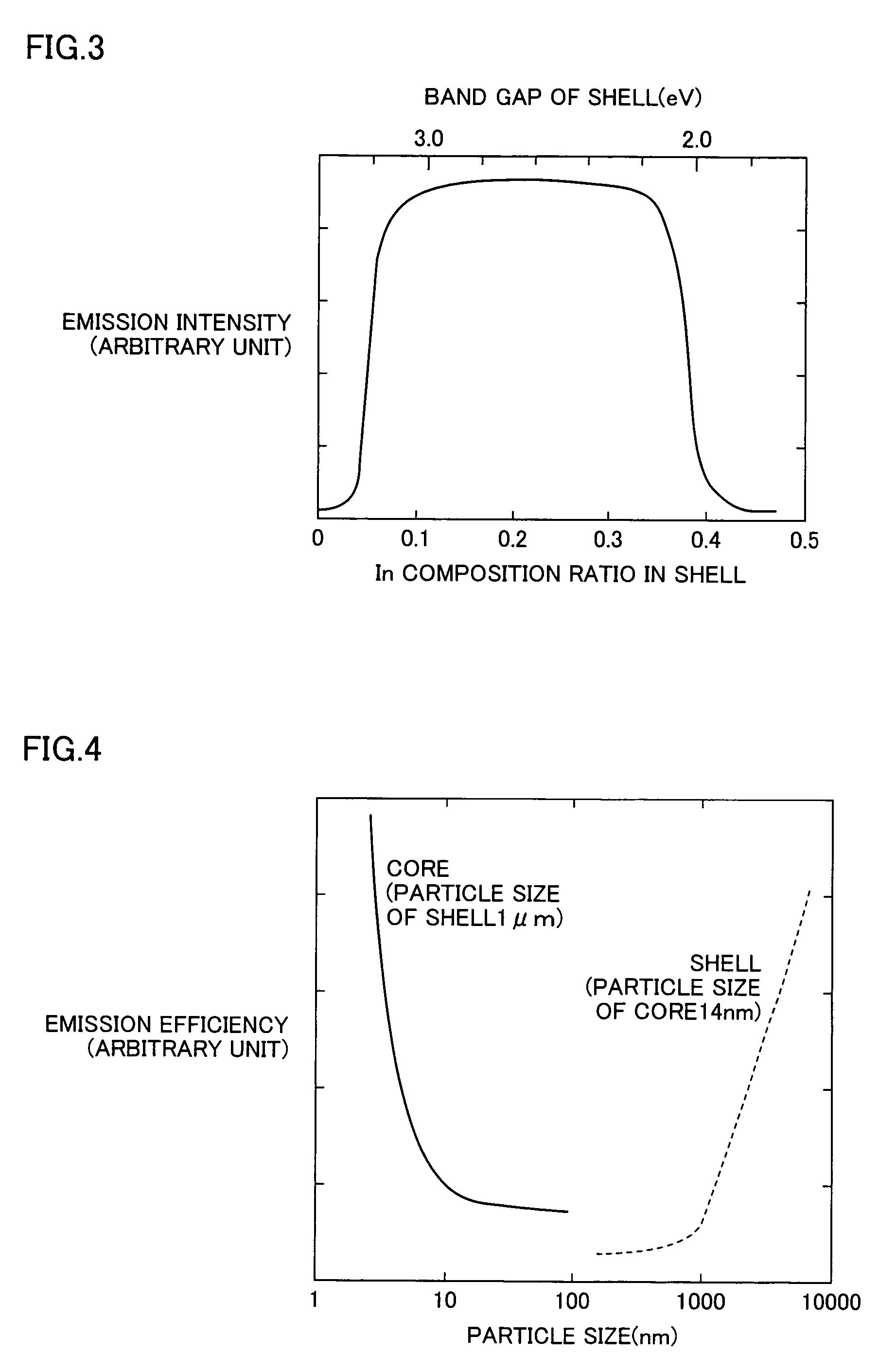
[0107]In the InGaN fluorescent material according to Example 2 obtained in the aforementioned manner, emission efficiency was not remarkably reduced but improved as compared with the InGaN fluorescent material according to Example 1 despite the particle size of not more than 1 μm of the shell.

example 3

[0108]According to Example 3, the present invention was applied to a green fluorescent material employing group III nitride semiconductors.

[0109]A fluorescent material (InGaN fluorescent material) comprising a two-layer structure of a core of In0.3Ga0.7N having a particle size of 10 nm and a shell of In0.1Ga0.9N having a particle size of 1.2 μm covering this core was prepared. Also according to Example 3, the InGaN fluorescent material was deposited on a sapphire substrate by laser ablation, similarly to Example 1. When the emission spectrum of the InGaN fluorescent material obtained in the aforementioned manner was measured, green emission of having a peak fluorescent wavelength of 530 nm was obtained.

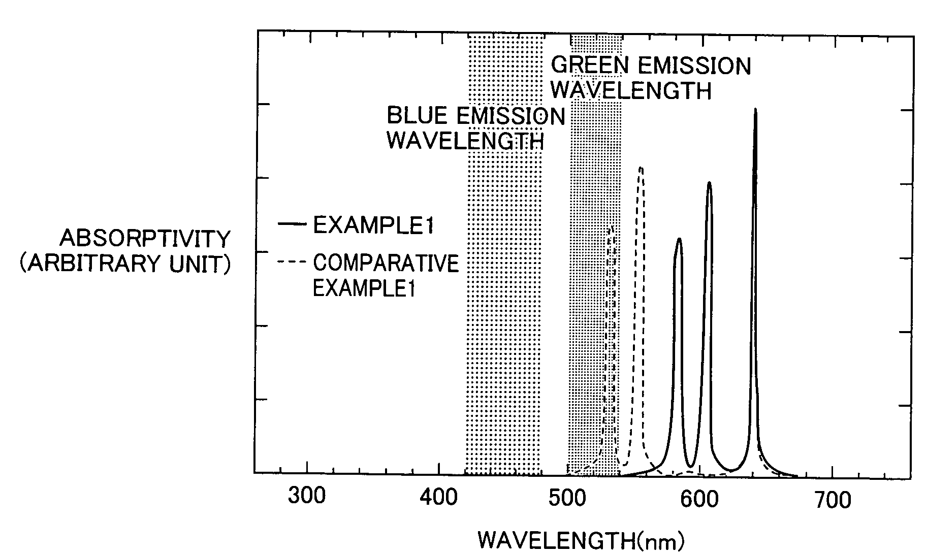
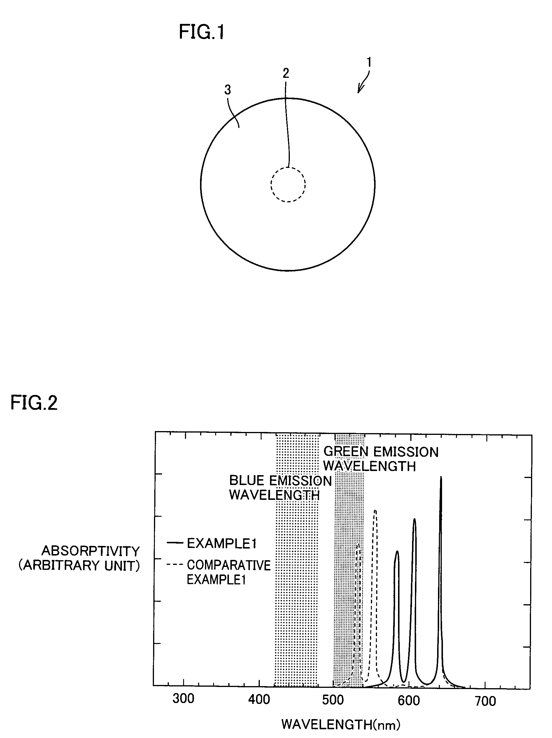
[0110]The InGaN fluorescent material according to Example 3 was color-mixed with blue and red light-emitting diodes having peak wavelengths of 450 nm and 625 nm respectively, for obtaining white emission. When the absorption spectrum of only the InGaN core constituting the InGaN fluor...


PUM

PropertyMeasurementUnit
high order energyaaaaaaaaaa
peak wavelengthaaaaaaaaaa

Abstract

A fluorescent material excellent in emission efficiency in white emission and a light-emitting apparatus employing this fluorescent material and having excellent color rendering are provided with a fluorescent material comprising a two-layer structure of a core of a particle size having a quantum effect and a shell covering this core in which the ground state energy of the core is in the range of 1.85 to 2.05 eV, the high order energy of the core is not in the ranges of 2.3 to 2.5 eV and 2.65 to 2.8 eV, or the ground state energy of the core is in the range of 2.3 to 2.5 eV, the high order energy of the core is not in the range of 2.65 to 2.8 eV an light-emitting apparatus employing these fluorescent materials.

Description

[0001]This nonprovisional application is based on Japanese Patent Application No. 2004-266939 filed with the Japan Patent Office on Sep. 14, 2004, the entire contents of which are hereby incorporated by reference.BACKGROUND OF THE INVENTION[0002]1. Field of the Invention[0003]The present invention relates to a fluorescent material and a light-emitting apparatus employing the same, and more specifically, it relates to a fluorescent material having a quantum effect and a light-emitting apparatus implementing white emission with the same. This light-emitting apparatus is preferably employed as an illuminator such as a backlight for a full-color display and a liquid crystal panel, for example.[0004]2. Description of the Background Art[0005]For example, Japanese Patent Laying-Open No. 11-340516 (1999) discloses an exemplary display and illuminator including fluorescent materials and a light-emitting device serving as a light source exciting the same. The aforementioned Japanese Patent La...

Claims


Application Information

Patent Timeline
Patent Type & Authority Patents(United States)
IPC IPC(8): H01J1/62C09K11/77H01L33/50H01L33/56H01S5/0232
CPCC09K11/02C09K11/62H01L33/502H01S5/005H01S5/02244Y10S977/774Y02B20/181H01L2924/0002H01L2924/00Y02B20/00H01S5/0225H01S5/0087H01S5/32341H01S5/0232
Inventor SAITO, HAJIMEMORIOKA, TATSUYAFUJITA, SHIZUOKAWAKAMI, YOICHIFUNATO, MITSURUHARADA, MASAFUMIFUJITA, LEGAL REPRESENTATIVE, KYOKOFUJITA, SHIGEO
Owner FUJITA SHIZUO
Why Eureka
Try Eureka