Quasi-plannar and FinFET-like transistors on bulk silicon

a silicon-like, quasi-plannar technology, applied in the field of semiconductor technology, can solve the problems of reducing gate control, reducing the ability of the gate to control whether the transistor is used, and reducing the control of the gate, so as to improve the control of the channel, improve the junction leakage, and improve the effect of channel width

Active Publication Date: 2009-07-21
TAIWAN SEMICON MFG CO LTD
View PDF3 Cites 137 Cited by
  • Summary
  • Abstract
  • Description
  • Claims
  • Application Information

AI Technical Summary

Benefits of technology

[0031]The present invention provides a combination of quasi-planar CMOS and FinFET-like transistor technology fabricated on bulk silicon wafers to bridge the gap between current planar CMOS to overcome scaling difficulties of short channel effects and future thin FinFET on SOI (to eliminate the “floating body effects”).
[0035]In another embodiment of the present invention, quasi-planar transistor channel is formed on a narrow and undoped silicon region between STI trenches, that allows the quasi-planar transistors to perform in a similar manner to a FinFet transistor having “thin body” effects. The raised source and drain provides advantages of reduced coupling between the source and drain, but there is an extra leakage path from the source and the drain to the bulk silicon. However, the present invention eliminates the “floating body effects” that occur in a FinFET on SOI device.
[0037]The present invention provides quasi-planar transistors having a doped channel with an enhanced channel width without increasing junction leakage. The gate wrapped over the edge fins and side-wall of the trench offers excellent control of the channel. Additionally, the source and drain is raised substantially above the side-wall of the trench channel, thereby significantly improving short-channel effects by suppressing the electrostatic coupling between the source and drain through the bulk silicon.

Problems solved by technology

Additionally, as CMOS transistors on bulk silicon are scaled to channel lengths below 100 nm, conventional CMOS transistors suffer from degraded performance as resulting from leakage currents that occur through channels, junctions, and gate dielectrics.
In particular, interactions between the source and drain of the CMOS device, typically results in both Vt roll-off and poor sub-threshold swing, degrade the ability of the gate to control whether the transistors is on or off.
As device size is scaled, however, this becomes increasingly difficult, since the distance between the source and drain is reduced, and hence, both the source and the drain increasingly interact with the channel, thus reducing gate control and increasing short channel effects (SCE).
SOI technology further improves the speed and reduces the operating power of the circuits.
The FinFET on SOI technology is generally superior to planar CMOS, however, the FinFET on SOI device has a quasi-planar surface that imposes significant challenges in processing including: providing a suitable SOI substrate, performing fine lithography, performing etching with a high aspect ratio, using a large tilt angle implant to produce a uniformly doped source and drain, and LDD regions.
Additionally, FinFET as any MOS transistors fabricated on SOI wafers suffer from a “floating body effect”.

Method used


Image

  • Quasi-plannar and FinFET-like transistors on bulk silicon
  • Quasi-plannar and FinFET-like transistors on bulk silicon
  • Quasi-plannar and FinFET-like transistors on bulk silicon

Examples


Embodiment Construction

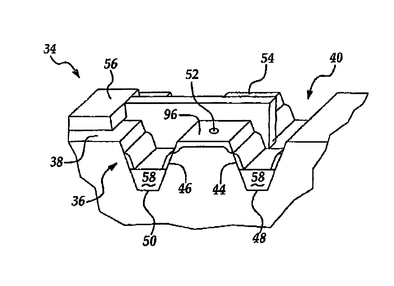
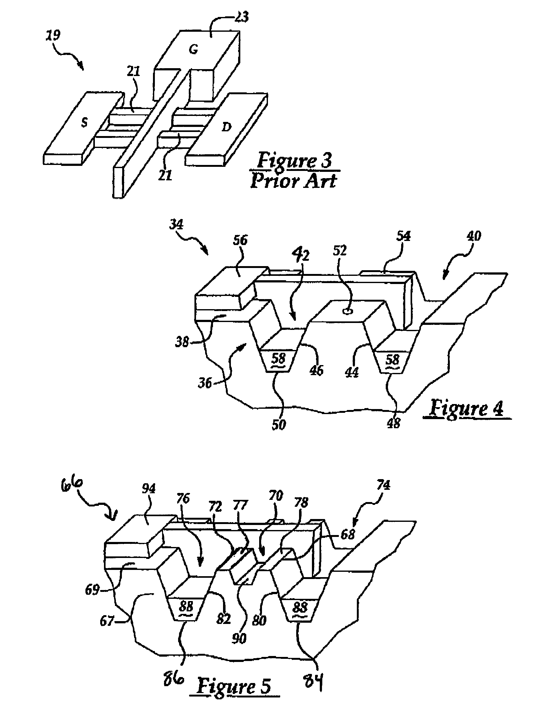
[0062]The present invention provides a combination of quasi-planar CMOS and FinFET-like transistor technology on bulk silicon that has improved device characteristics and performance over that of planar CMOS and FinFET on SOI technologies.

[0063]In general, a semiconductor substrate is provided. Preferably, the substrate is a silicon material. The substrate has at least one, but preferably two recessed regions or “STI trenches” formed therewithin, each having a side-wall and a bottom portion, each bottom portion having a bottom wall. The two STI trenches are spaced apart by a top surface (or top wall) of the silicon substrate, wherein the channel of the active region is defined by the top wall of the silicon substrate and the two side-walls of each trench, wherein each of the side-walls is juxtaposed to an edge of an active area of the transistor.

[0064]A source and a drain of the transistor device are disposed on the top wall of the silicon substrate between each of the two shallow t...


PUM


Abstract

The types of quasi-planar CMOS and FinFET-like transistor devices on a bulk silicon substrate are disclosed. A first device has a doped and recessed channel formed in a shallow trench sidewall. A second device has a doped, recessed channel and has a plurality of edge-fins juxtaposed on an edge of an active region of the device. A third device has an undoped recessed channel formed in a sidewall of a shallow trench, wherein the undoped recessed channel further has a plurality of edge-fins disposed thereon. Additionally, an extra mask may be added to each device to allow for fabrication of both conventional transistors and FinFET-like transistors on bulk silicon. The extra mask may protect the source and drain areas from recess etching of the silicon substrate. Several methods of fabricating each device are also disclosed.

Description

RELATED APPLICATION[0001]This is a utility application of provisional application no. 60 / 565,038, filed Apr. 24, 2004.FIELD OF THE INVENTION[0002]The present invention generally relates to FinFET technology and more particularly, relates to quasi-planar CMOS and FinFET-like transistors fabricated on bulk silicon wafers (referred to as bulk-FinFET or FinFET-on-bulk) with enhanced drive current and suppressed short-channel effects and associated fabrication methods.BACKGROUND[0003]Performance enhancement between generations of conventional CMOS integrated circuit is generally achieved by applying shorter gate length and thinner gate oxide in MOS transistors fabricated on bulk or silicon-on-oxide (SOI) wafers. This is generally referred to as the “scaling” of MOS transistors.[0004]Metal-Oxide-Semiconductor-Field-Effect-transistors (MOSFETs), having a source, a drain region, and a gate electrode formed using a gate oxide, are commonly used in IC devices. As the gate oxide becomes thinne...

Claims


Application Information

Patent Timeline
Patent Type & Authority Patents(United States)
IPC IPC(8): H01L27/088H01L21/00H01L21/336H01L29/786
CPCH01L29/7853H01L29/66795
Inventor CHI, MIN-HWACHIANG, WEN-CHUANCHIANG, MU-CHI
Owner TAIWAN SEMICON MFG CO LTD
Why Eureka
Try Eureka