Nitrogen treatment to improve high-k gate dielectrics

a dielectric and high-k gate technology, applied in the field of nitrogen treatment to improve the performance of high-k gate dielectrics, can solve the problems of affecting device performance, other deleterious effects on the underlying substrate, and increasing the leakage current of higher gate dielectrics

Active Publication Date: 2009-07-21
TAIWAN SEMICON MFG CO LTD
View PDF33 Cites 12 Cited by
  • Summary
  • Abstract
  • Description
  • Claims
  • Application Information

AI Technical Summary

Benefits of technology

[0008]These and other problems are generally solved or circumvented, and technical advantages are generally achieved by preferred embodiments of the present invention that provide a novel process and structure for semiconductor devices using high-k gate dielectric materials. Preferred embodiments of the invention provide a multilayer dielectric stack and method, wherein the nitrogen distribution in the gate dielectric overcomes manufacturing and reliability problems.

Problems solved by technology

One approach is to decrease the thickness of the silicon dioxide gate dielectric, which will increase higher gate dielectric leakage current.
Well known phenomena of the silicon oxide gate dielectric that can deleteriously affect device performance include charge traps such as intrinsic and extrinsic defects throughout the oxide layer, and so-called interface states at the oxide-silicon interface resulting from silicon dangling bonds.
A nitrided oxide layer (or any nitrogen containing dielectric), however, may have other deleterious affects on the underlying substrate, such as nitrogen diffusion into the substrate, and poor device characteristics due to nitrogen-incorporated dopant diffusion or dopant deactivation in a source / drain and their extensions.
Particularly, negative bias temperature instability (NBTI) may be adversely impacted by the presence of a nitrogen containing material in contact with the substrate (and more particularly in contact with the channel region).
While the beneficial affects of a nitrided gate electrode (such as reduced charge trap sites) may outweigh the negative effects for some transistor applications, such as core logic devices, the deleterious effects are more significant for other applications such as input / output (I / O) devices.

Method used


Image

  • Nitrogen treatment to improve high-k gate dielectrics
  • Nitrogen treatment to improve high-k gate dielectrics
  • Nitrogen treatment to improve high-k gate dielectrics

Examples


Embodiment Construction

[0019]The operation and fabrication of the presently preferred embodiments are discussed in detail below. However, the embodiments and examples described herein are not the only applications or uses contemplated for the invention. The specific embodiments discussed are merely illustrative of specific ways to make and use the invention, and do not limit the scope of the invention or the appended claims.

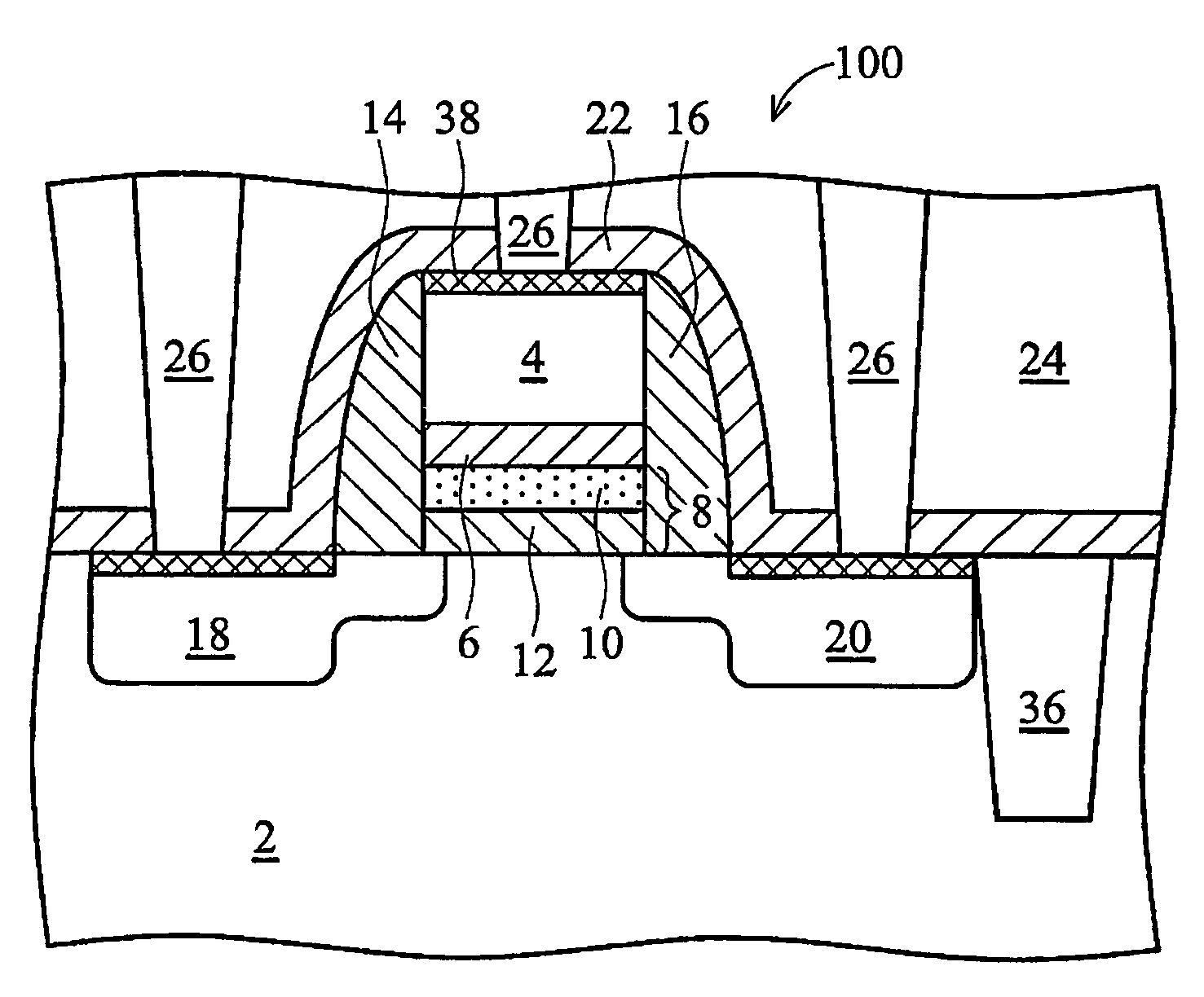
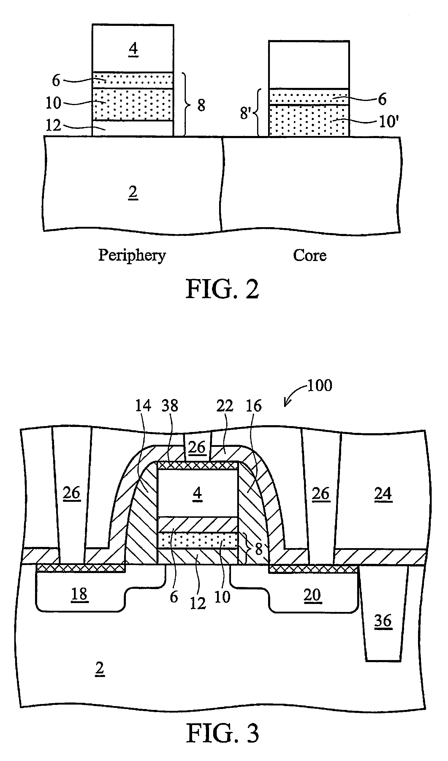
[0020]Shown in FIG. 1 is a semiconductor substrate 2 employed within a microelectronics fabrication. Semiconductor substrate 2 is preferably a silicon wafer, however, substrate 2 may comprise Ge, SiGe, strained silicon, strained germanium, GaAs, silicon on insulator (SOI), SiGeOI, GeOI, a stacked arrangement of layers such as Si / SiGe, and a combination thereof. In some example, 110> or 100> channel orientation may be applied in the substrate. The silicon substrate 2 is employed within a microelectronics fabrication chosen from the group including but not limited to integrated circuit m...


PUM

PropertyMeasurementUnit
dielectric constantaaaaaaaaaa
thicknessaaaaaaaaaa
thicknessaaaaaaaaaa

Abstract

A MOSFET having a nitrided gate dielectric and its manufacture are disclosed. The method comprises providing a substrate and depositing a non-high-k dielectric material on the substrate. The non-high-k dielectric comprises two layers. The first layer adjacent the substrate is essentially nitrogen-free, and the second layer includes between about 1015 atoms / cm3 to about 1022 atoms / cm3 nitrogen. The MOSFET further includes a high-k dielectric material on the nitrided, non-high-k dielectric. The high-k dielectric preferably includes HfSiON, ZrSiON, or nitrided Al2O3. Embodiments further include asymmetric manufacturing techniques wherein core and peripheral integrated circuit areas are separately optimized.

Description

[0001]This application claims the benefit of U.S. Provisional Application No. 60 / 637,599 filed on Dec. 20, 2004, entitled Nitrogen Treatment to Improve High-K Gate Dielectrics, which application is hereby incorporated herein by reference.TECHNICAL FIELD[0002]This invention relates generally to semiconductor devices and methods of manufacturing same. More particularly, this invention relates to an improved input / output transistor device having a composite gate dielectric comprising a nitrogen containing, high-k dielectric, and an underlying dielectric layer having a nitrogen containing portion in contact with the high-k dielectric layer and a non-nitrogen containing portion that is in contact with the substrate.BACKGROUND[0003]Gate dielectric performance and reliability is an ongoing concern in conventional CMOS processing. This concern is particularly significant as device geometries shrink to the sub-micron realm (e.g., 90 nm, 65 nm, and below) and as device reliability standards a...

Claims


Application Information

Patent Timeline
Patent Type & Authority Patents(United States)
IPC IPC(8): H01L21/8238
CPCH01L21/28202H01L21/76829H01L21/823462H01L21/823857H01L29/513H01L29/7843H01L29/518H01L29/665H01L29/6659H01L29/7833H01L29/517
Inventor WANG, CHIH-HAOWANG, TA-WEICHEN, SHANG-CHIHTSAI, CHING-WEI
Owner TAIWAN SEMICON MFG CO LTD
Why Eureka
Try Eureka