Wafer level package having a stress relief spacer and manufacturing method thereof

a stress relief spacer and packaging technology, applied in the direction of semiconductor devices, semiconductor/solid-state device details, electrical apparatus, etc., can solve the problems of large mismatch, damage to the via, and negatively affecting the device yield during manufacture, so as to improve the device yield and device reliability, and the effect of avoiding cracking and delamination

Active Publication Date: 2009-08-11
SAMSUNG ELECTRONICS CO LTD
View PDF7 Cites 16 Cited by
  • Summary
  • Abstract
  • Description
  • Claims
  • Application Information

AI Technical Summary

Benefits of technology

[0005]The present invention is directed to a semiconductor device package having a stress relief spacer, and a manufacturing method thereof. Metal fingers that extend from the body of a chip provide for chip interconnection. The metal fingers are isolated from the body of the chip by a stress-relief spacer. In one example, such isolation takes the form of an air gap. In another example, such isolation takes the form of an elastomer material. In either case, CTE mismatch between the metal interconnect fingers and the body of the chip is avoided, alleviating the problems associated with cracking and delamination. This leads to an improvement in device yield and device reliability.

Problems solved by technology

Such stress is typically caused by a mismatch in coefficient of thermal expansion (CTE) between two adjacent layers.
In this situation, during device fabrication, or later during device operation, heating and cooling processes can cause damage to the via.
This is often times due to the CTE mismatch between the layers.
For example, silicon has a CTE value of 3, while the dielectric layer can have a CTE value on the order of 50-60; resulting in a large mismatch.
Such mismatch can cause cracking and delamination when subjected to numerous heating and cooling thermal cycles, negatively affecting device yield during manufacture, and device reliability during operation.

Method used


Image

  • Wafer level package having a stress relief spacer and manufacturing method thereof
  • Wafer level package having a stress relief spacer and manufacturing method thereof
  • Wafer level package having a stress relief spacer and manufacturing method thereof

Examples


first embodiment

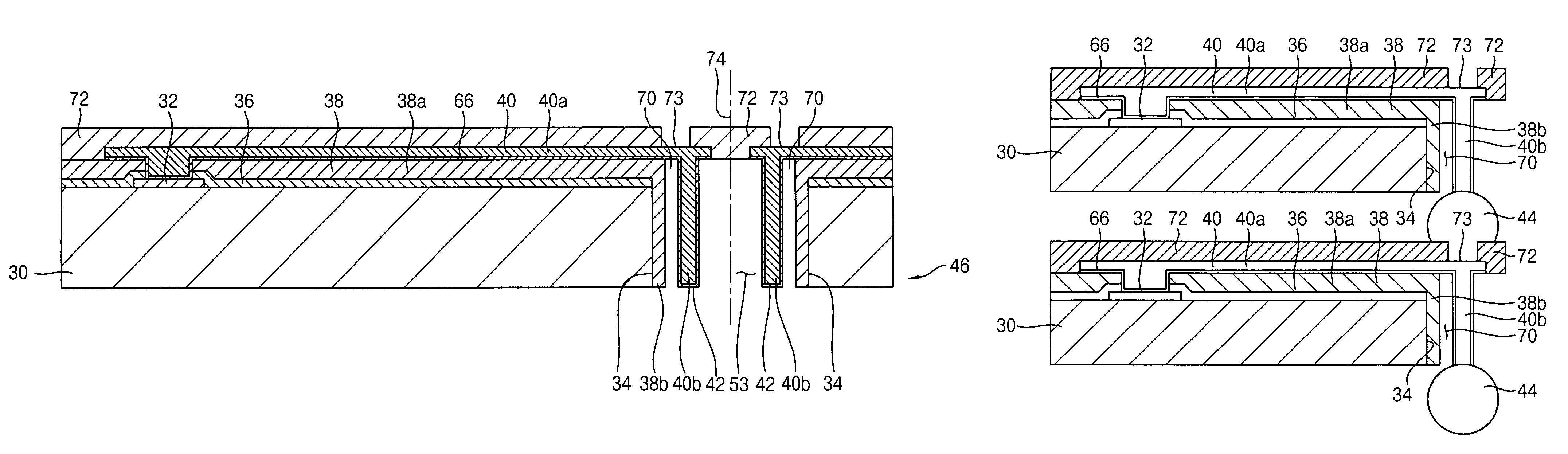
[0064]FIGS. 2 through 12 are sectional views of a method for fabricating a wafer level package (WLP) in accordance with the present invention.

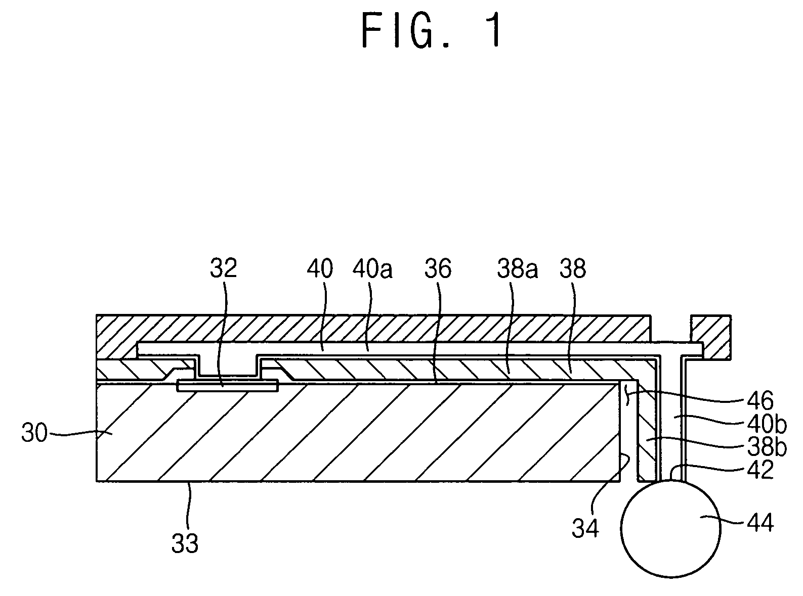
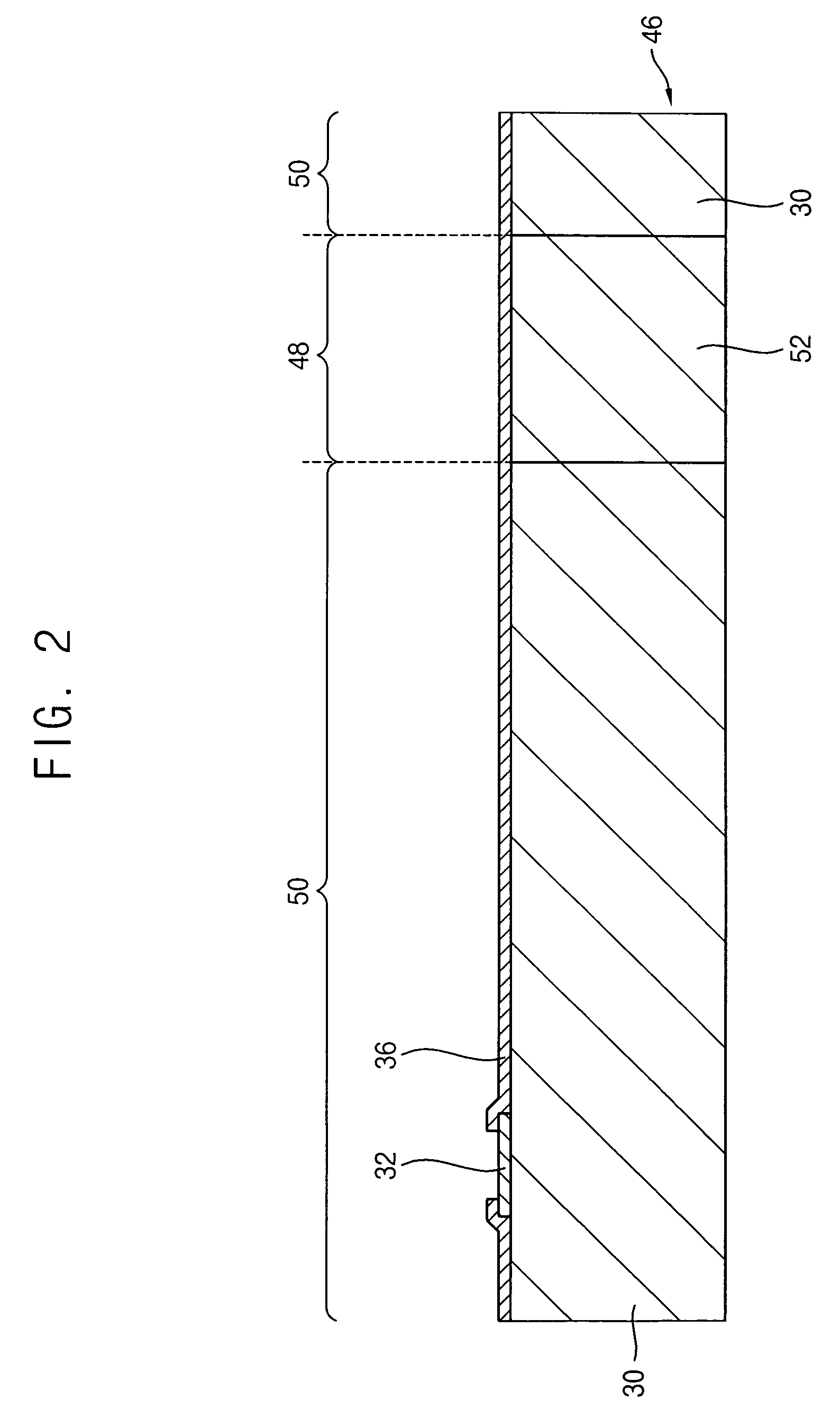
[0065]Referring to FIG. 2, a semiconductor wafer 46 is partitioned by a scribe lane 52 into neighboring device regions 50 and scribe lane regions 48. Adjacent dies of the wafer share a common scribe lane 52, which, when fully scribed, or cut, separates the wafers into individual dies. A bonding pad 32, or other conductive feature of the device, is provided in the device region 50. An oxide layer pattern 36, for example comprising silicon oxide or silicon nitride, is formed on a top surface of the substrate, and is patterned to expose the bonding pad 32. The oxide layer pattern 36 is provided as a passivation layer to protect a cell region of the device during fabrication.

[0066]Referring to FIG. 3, the scribe lane 52 is partially diced, or partially removed, to form a first opening 53 so that a lower portion of the substrate 30 body remains in ...

second embodiment

[0079]FIGS. 13 through 20 are sectional views of a method for fabricating a wafer level package (WLP) in accordance with the present invention.

[0080]Referring to FIG. 13, the substrate of the present second embodiment is prepared in the same manner as that of the first embodiment as shown in FIG. 2. As in the first embodiment, the scribe lane 52 of the second embodiment is partially diced, or removed, to form a first opening 53 so that a lower portion of the substrate 30 body remains in the scribe lane 52. In one example, the scribe lane 52 is partially diced to a depth that corresponds with the eventual desired length of the vertical portions 40b of the conductive interconnects 40 (see FIG. 20, below). An outer edge 34 of the die is exposed by the partial dicing of the scribe lane 52 in the opening 53. A first photoresist layer is then formed in the first opening 53 and is patterned to provide a first photoresist layer pattern 82 including a second opening 84. In a case where the s...

third embodiment

[0089]FIGS. 21 and 22 are sectional views of a method for fabricating a wafer level package (WLP) in accordance with the present invention.

[0090]The embodiment of FIG. 21 is similar in structure to the first embodiment as depicted in FIG. 11, in that the vertical portion 38b of the dielectric layer pattern 38 lies directly on the outer edge 34 of the substrate 30, and the vertical portions 40b of the conductive interconnects 40 are spaced apart from the vertical portion 38b of the dielectric layer pattern 38. However, in the present embodiment of FIG. 21, the air gap, or void, between each vertical portion 40b of the conductive interconnect 40 and the vertical portion 38b of the dielectric layer pattern 38 is filled with an elastomer material 92. The elastomer material 92 can be provided following removal of the first photoresist layer pattern 62 occupying the first opening 53, as described above in conjunction with FIG. 10. Alternatively, the elastomer material 92 can be provided a...


PUM


Abstract

In a semiconductor device package having a stress relief spacer, and a manufacturing method thereof, metal interconnect fingers extend from the body of a chip provide for chip interconnection. The metal fingers are isolated from the body of the chip by a stress-relief spacer. In one example, such isolation takes the form of an air gap. In another example, such isolation takes the form of an elastomer material. In either case, mismatch in coefficient of thermal expansion between the metal interconnect fingers and the body of the chip is avoided, alleviating the problems associated with cracking and delamination, and leading to improved device yield and device reliability.

Description

RELATED APPLICATIONS[0001]This application claims priority under 35 U.S.C. 119 to Korean Patent Application No. 10-2006-0000786 filed on Jan. 4, 2006, the content of which is incorporated herein by reference in its entirety.FIELD OF THE INVENTION[0002]The present invention relates to a semiconductor device package including a stress relief mechanism, and manufacturing methods thereof.BACKGROUND OF THE INVENTION[0003]Semiconductor manufacturing and packaging technology has evolved to the point where device packages can include multiple integrated circuit chips in a stacked relationship in order to provide a smaller form factor and higher integration density at the package level. In such packages, the individual chips each include a multitude of signals that are to be externally transferred. Such transfer occurs over a plurality of metal interconnects that distribute signals to an end surface of the chip. The metal interconnects of different chips in the stack are connected according ...

Claims


Application Information

Patent Timeline
Patent Type & Authority Patents(United States)
IPC IPC(8): H01L21/00H01L21/44
CPCH01L21/76898H01L23/481H01L25/0657H01L25/50H01L2224/13025H01L2224/274H01L2224/0401H01L2225/06541H01L2924/01079H01L2924/01087H01L2224/02371H01L2224/02372H01L2225/06513H01L23/12
Inventor CHUNG, HYUN-SOOLEE, HO-JINJANG, DONG-HYUNLEE, DONG-HO
Owner SAMSUNG ELECTRONICS CO LTD
Why Eureka
Try Eureka