Method and structure for reducing induced mechanical stresses

a mechanical stress and mechanical stress technology, applied in the field of semiconductors, can solve the problems of affecting the performance of the nfet, requiring numerous additional processing steps, time-consuming and expensive, and requiring additional materials, etc., to avoid degradation of the performance of the second fet device, and improve the performance of the first fet device

Inactive Publication Date: 2009-08-11
TAIWAN SEMICON MFG CO LTD
View PDF9 Cites 2 Cited by
  • Summary
  • Abstract
  • Description
  • Claims
  • Application Information

AI Technical Summary

Benefits of technology

[0009]It is another object of the present invention to provide methods and structures that significantly reduce processing complexity in removing induced mechanical stresses, while avoiding degradation of FET performance.
[0010]A further object of the invention is to provide methods and structures for easily and cost effectively selectively removing stressed liners.
[0011]Another object of the invention is to provide methods and structures for providing compression in the longitudinal orientation, for the PFET, while mitigating the NFET degradation by substantially reducing the vertical stress induced by the stress liner.
[0013]The above and other objects, which will be apparent to those skilled in the art, are achieved in the present invention, which is directed to a method of relieving stresses in stressed semiconductor liners. The method includes providing a semiconductor structure having a first and second FET, followed by providing and depositing a stress liner that enhances performance of the first FET over an entire surface of the semiconductor structure. A disposable layer is then deposited over the single stress liner, which is then recessed to expose only the upper portion of the single stress liner only over at least the second FET. This exposed single stress liner is removed from over the at least second FET to expose a top surface of a gate of the second FET. Any remaining portions of the disposable layer are then removed, thereby enhancing performance of the first FET while avoiding degradation of the second FET.
[0017]Another method of the invention is for relieving stresses in stressed semiconductor liners. This method includes providing a semiconductor structure having an NFET and a PFET, followed by providing and depositing a stress liner that enhances performance of either the NFET or the PFET. This stress liner covers both the NFET and PFET. A disposable layer is deposited to entirely cover the single stress liner and both the NFET and the PFET. This disposable layer is then selectively recessed to expose only the single stress liner over a gate of the NFET or the PFET that is not enhanced by the deposited single stress liner. The exposed single stress liner is then removed to expose a top surface of the gate. Any remaining portions of the disposable layer are then removed. This method enhances performance of either the NFET or the PFET, while avoiding degradation of the NFET or the PFET that is not enhanced by the single stress liner.
[0019]In still another aspect, the invention is directed to an intermediate semiconductor structure that includes a semiconductor structure having first and second FET devices, respectively, having first and second gates. In this intermediate product, a single stress liner resides over a surface of the semiconductor structure, over the first FET gate, and not over the second FET gate. In so doing, the single stress liner enhances performance of the first FET device while avoiding degradation of performance of the second FET device. The single stress liner may be a tensile stress liner when the first FET is an NFET and the second FET is a PFET on an (011) oriented silicon surface. Alternatively, the single stress liner may be a compressive stress liner when the first FET is a PFET on an (001) oriented silicon surface and the second FET is a NFET.

Problems solved by technology

Again, this is because the type of stress that is beneficial for the performance of an NFET is generally disadvantageous for the performance of the PFET formed in the same substrate.
While these methods do provide structures that have tensile stresses being applied to the NFET device and the compressive stresses being applied along the longitudinal direction of the PFET device, they often require numerous additional processing steps, additional materials, and / or more complex processing.
Overall, the disadvantages of the prior art approaches is that they are time consuming and expensive.

Method used


Image

  • Method and structure for reducing induced mechanical stresses
  • Method and structure for reducing induced mechanical stresses
  • Method and structure for reducing induced mechanical stresses

Examples


Embodiment Construction

)

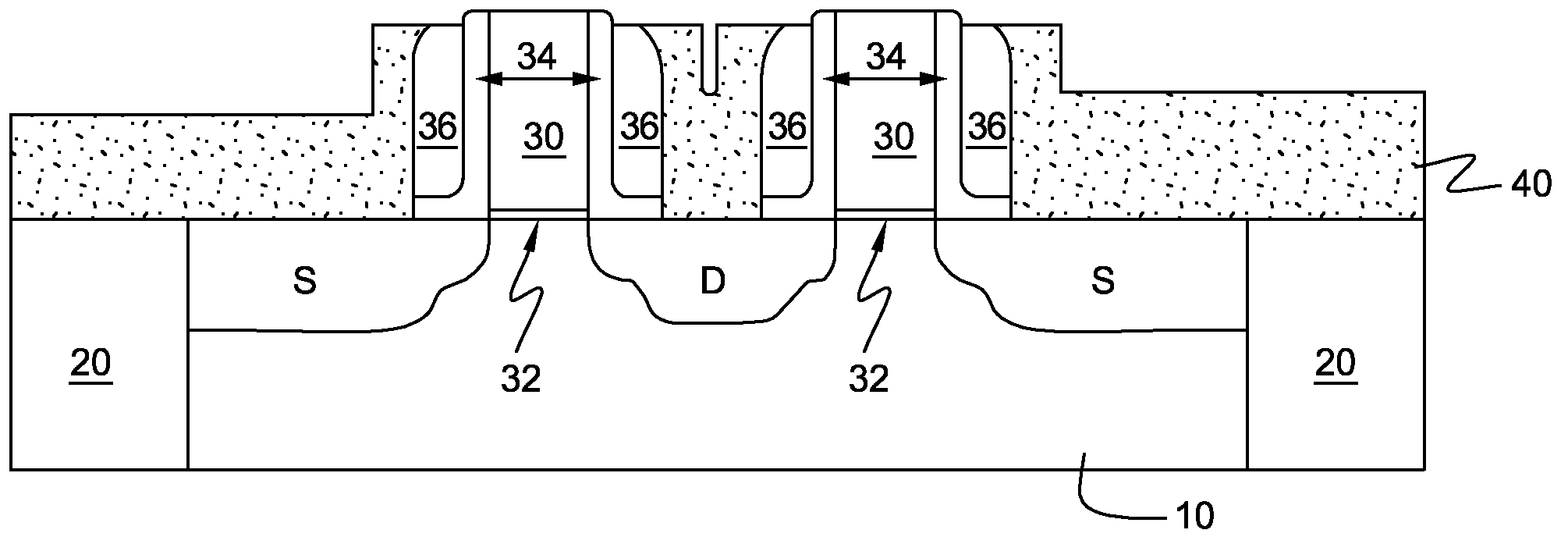
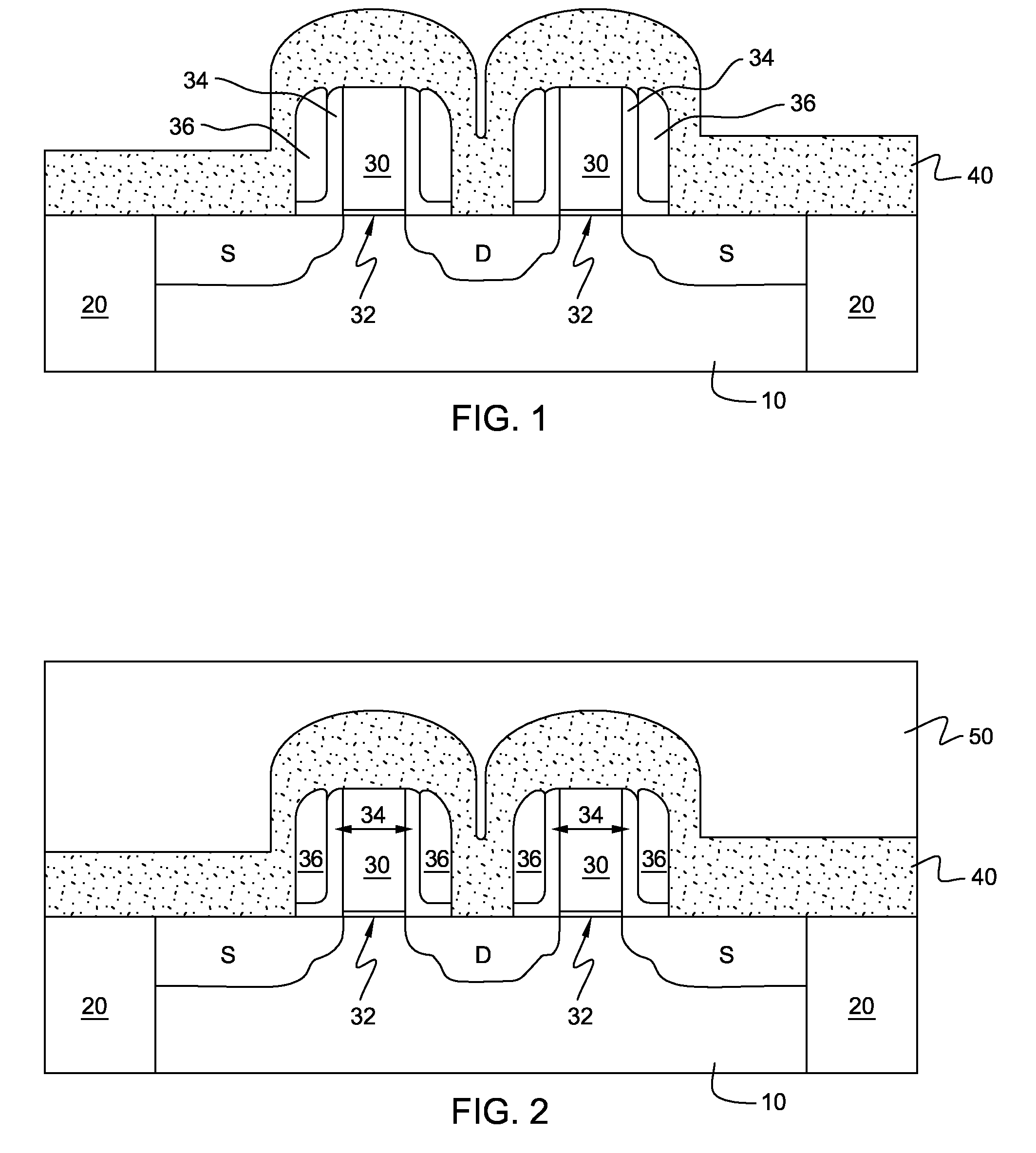
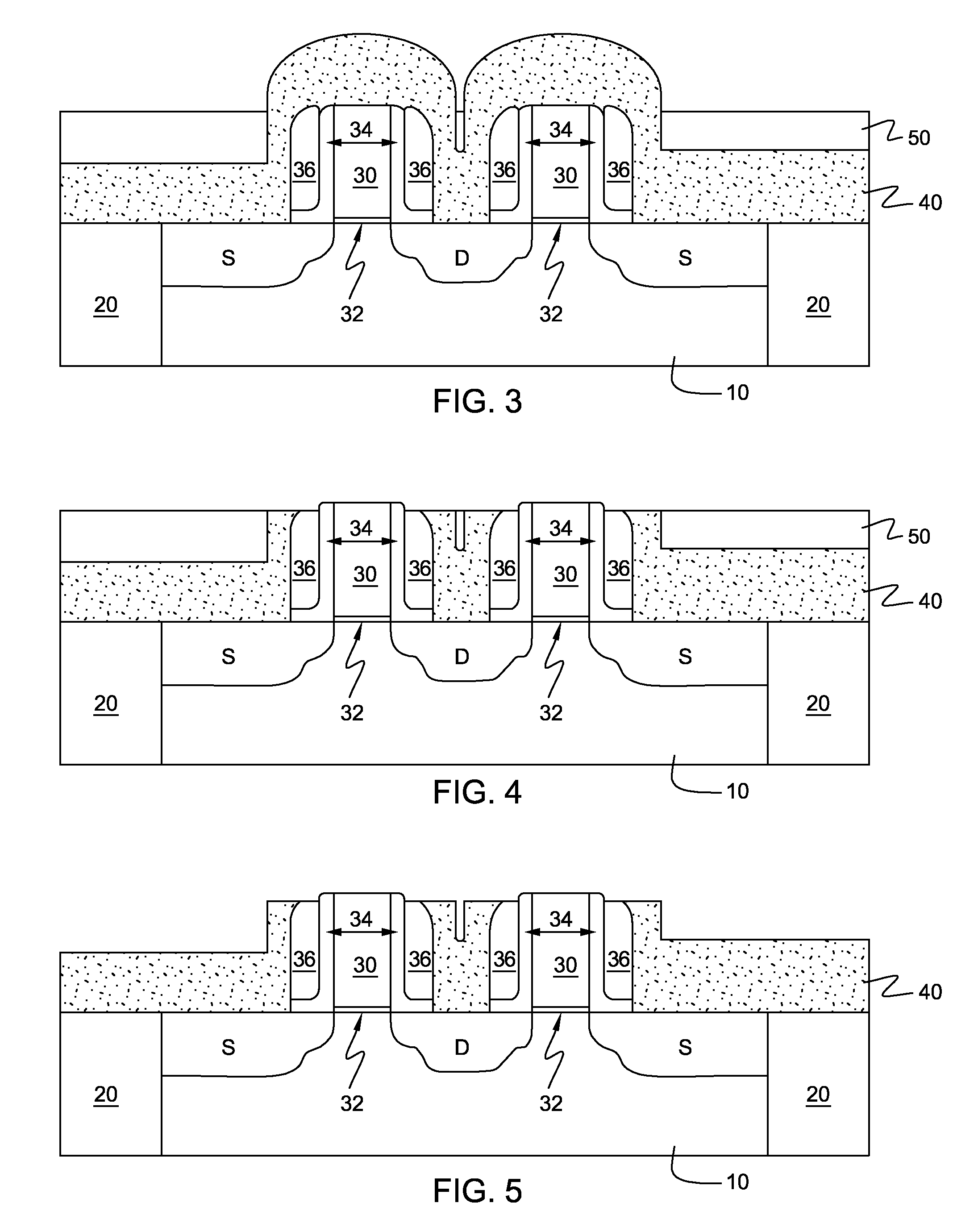
[0024]In describing the preferred embodiment of the present invention, reference will be made herein to FIGS. 1-8 of the drawings in which like numerals refer to like features of the invention.

[0025]Referring to the drawings, FIG. 1 shows a cross sectional view of a portion a semiconductor device having a transistor body with a pair of NFET devices. The semiconductor is formed by conventional techniques using a substrate 10 of any known material including silicon, strained silicon, silicon germanium, germanium, silicon on insulator, or any other semiconductor substrate. An isolation device 20, such as shallow trench isolation (STI), is formed on the substrate 10 for defining n-well and p-well regions of the substrate.

[0026]A gate dielectric 32 along with the gate electrodes 30 are formed over the substrate by known techniques. For instance, first a gate dielectric layer is grown or deposited over the substrate followed by deposition of a semiconductor, metal, or silicide material (...


PUM


Abstract

Methods and structures for relieving stresses in stressed semiconductor liners. A stress liner that enhances performance of either an NFET or a PFET is deposited over a semiconductor to cover the NFET and PFET. A disposable layer is deposited to entirely cover the stress liner, NFET and PFET. This disposable layer is selectively recessed to expose only the single stress liner over a gate of the NFET or PFET that is not enhanced by such stress liner, and then this exposed liner is removed to expose a top of such gate. Remaining portions of the disposable layer are removed, thereby enhancing performance of either the NFET or PFET, while avoiding degradation of the NFET or PFET not enhanced by the stress liner. The single stress liner is a tensile stress liner for enhancing performance of the NFET, or it is a compressive stress liner for enhancing performance of the PFET.

Description

BACKGROUND OF THE INVENTION[0001]1. Field of the Invention[0002]The present invention relates to semiconductors, and in particular, to methods and structures for selectively removing stressed liners to relieve mechanical stresses.[0003]2. Description of Related Art[0004]It is known that mechanical stresses can modulate performance of a semiconductor device, such as, a metal-oxide-semiconductor field effect transistor (MOSFET), for enhancing the characteristics thereof. In particular, it is known that the electron mobility of an n-type MOSFET (NFET) formed on silicon with a (001) surface orientation is enhanced when tensile stress is applied in the direction of current flow (e.g. longitudinal stress) and / or in the direction perpendicular to, but in the plane of current flow (e.g. transverse stress), and / or when compressive stress is applied in the direction normal to the plane of current flow (e.g. vertical stress) in the MOSFET channel. In addition, it is known that the hole mobilit...

Claims


Application Information

Patent Timeline
Patent Type & Authority Patents(United States)
IPC IPC(8): H01L21/337
CPCH01L21/823412H01L29/7843H01L21/823425H01L29/6653
Inventor GREENE, BRIAN J.RENGARAJAN, RAJESH
Owner TAIWAN SEMICON MFG CO LTD
Why Eureka
Try Eureka