Light emitting device

a technology light source, which is applied in the direction of semiconductor devices, diodes, electrical apparatus, etc., can solve the problems of significant reduction in the yield complicated manufacturing process of light emitting device, and unnecessary backlight used in liquid crystal display

Inactive Publication Date: 2009-08-25
SEMICON ENERGY LAB CO LTD
View PDF55 Cites 105 Cited by
  • Summary
  • Abstract
  • Description
  • Claims
  • Application Information

AI Technical Summary

Benefits of technology

[0012]According to the present invention, since a manufacturing process for forming the light emitting device and a manufacturing process for forming the colored layer are individually performed, such an advantage is obtained that the yield of the photolithography process for forming the colored layer does not influence the manufacturing process for forming the light emitting device.

Problems solved by technology

Since the EL light emitting device is a display device using a self light emitting element, a back light which may be used in a liquid crystal display is unnecessary.
However, when the photolithography process is performed three times, there arose problems in that not only a manufacturing process of the EL light emitting device is complicated, but also a significant reduction in its yield may be caused, because the yield of individual photolithography process influences by multiplication.
As a result, an increase of a manufacturing cost due to the reduction in the yield and an extension of a manufacturing period became a problem.

Method used


Image

  • Light emitting device
  • Light emitting device
  • Light emitting device

Examples


embodiment 1

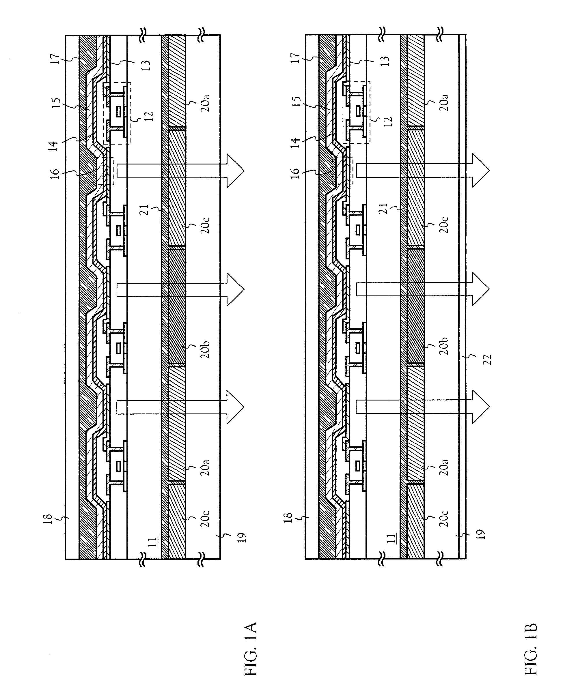
[0056]In this embodiment, the case where the present invention is applied to a passive matrix type (simple matrix type) EL light emitting device will be described. Note that reference numerals identical to those used in FIGS. 1A and 1B may be referred to the descriptions in embodiment mode.

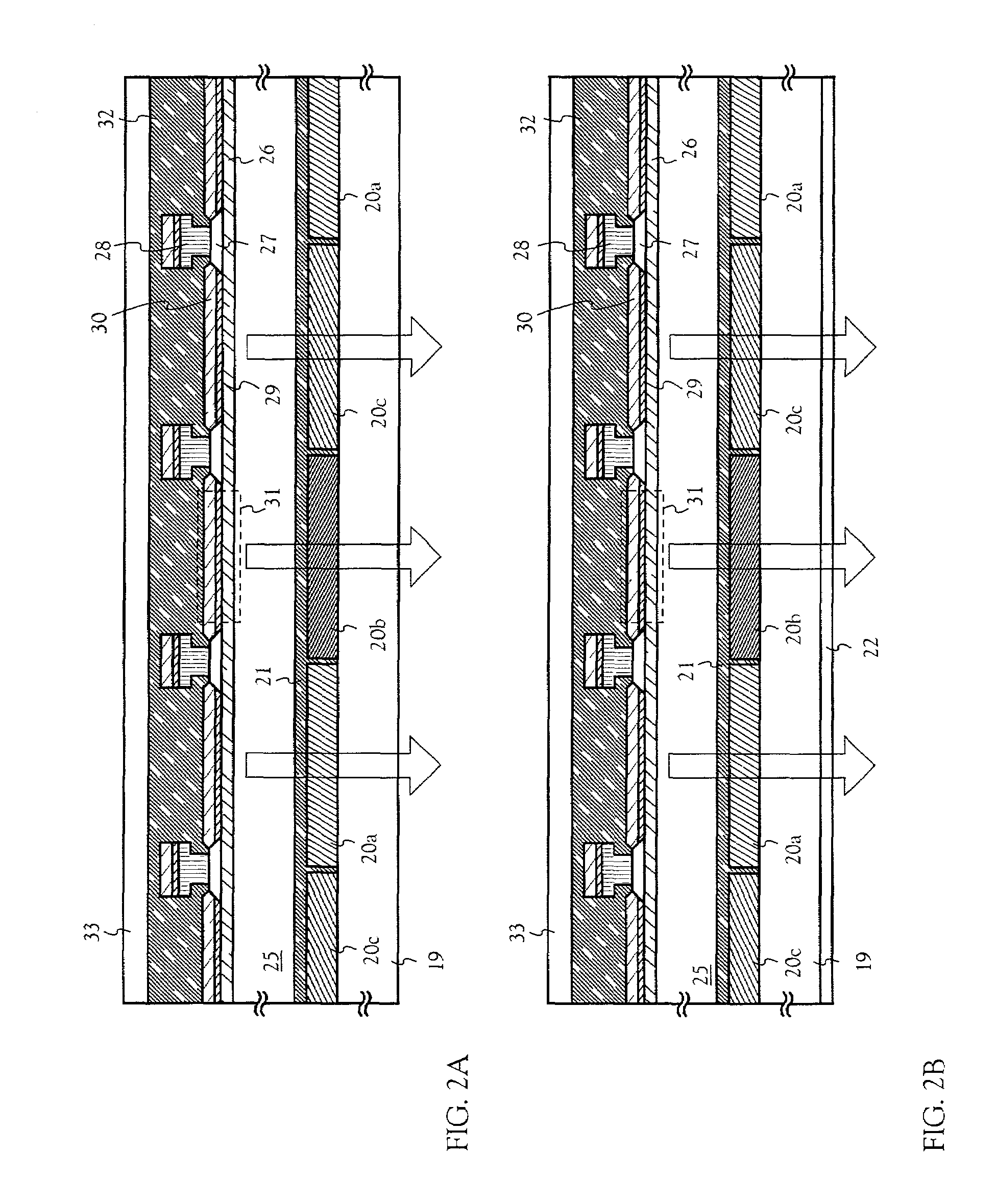
[0057]In FIG. 2A, reference numeral 25 denotes a glass substrate, and reference numeral 26 is an anode made of an oxide conductive film. In this embodiment, a compound film made of indium oxide and tin oxide is used as the oxide conductive film. Note that, in the anode 26, plural rectangular electrodes in which a direction from the left to the right in the paper is a longitudinal direction, are provided along a depth direction in the paper.

[0058]Also, a first bank member 27 and a second bank member 28, which are made from an insulating film are provided on the anode 26. In this embodiment, a silicon oxide film is used as the first bank member 27, and a resin film is used as the second bank member ...

embodiment 2

[0063]In the light emitting device as shown in FIGS. 1A and 1B or FIGS. 2A and 2B, after the active matrix substrate is completed, it is effective that the substrate on which an element has been formed is polished using a known CMP (chemical mechanical polishing) technique to make a thickness of the substrate thin. FIGS. 3A and 3B show a light emitting device according to this embodiment. Note that reference numerals identical to those used in FIGS. 1A and 1B or FIGS. 2A and 2B may be referred to the descriptions of embodiment mode.

[0064]In FIG. 3A, reference numeral 35 denotes a substrate polished by using the CMP technique, a structure except for this is similar to that of FIG. 1B. In this embodiment, a thickness of the substrate 35 is set as 300 μm or less (typically, 100 to 300 μm) by using the CMP technique. It is effective, for improving directivity of light, to make the thickness is set as a pixel pitch (distance from one pixel to next pixel) or less.

[0065]Also, FIG. 3B is an...

embodiment 3

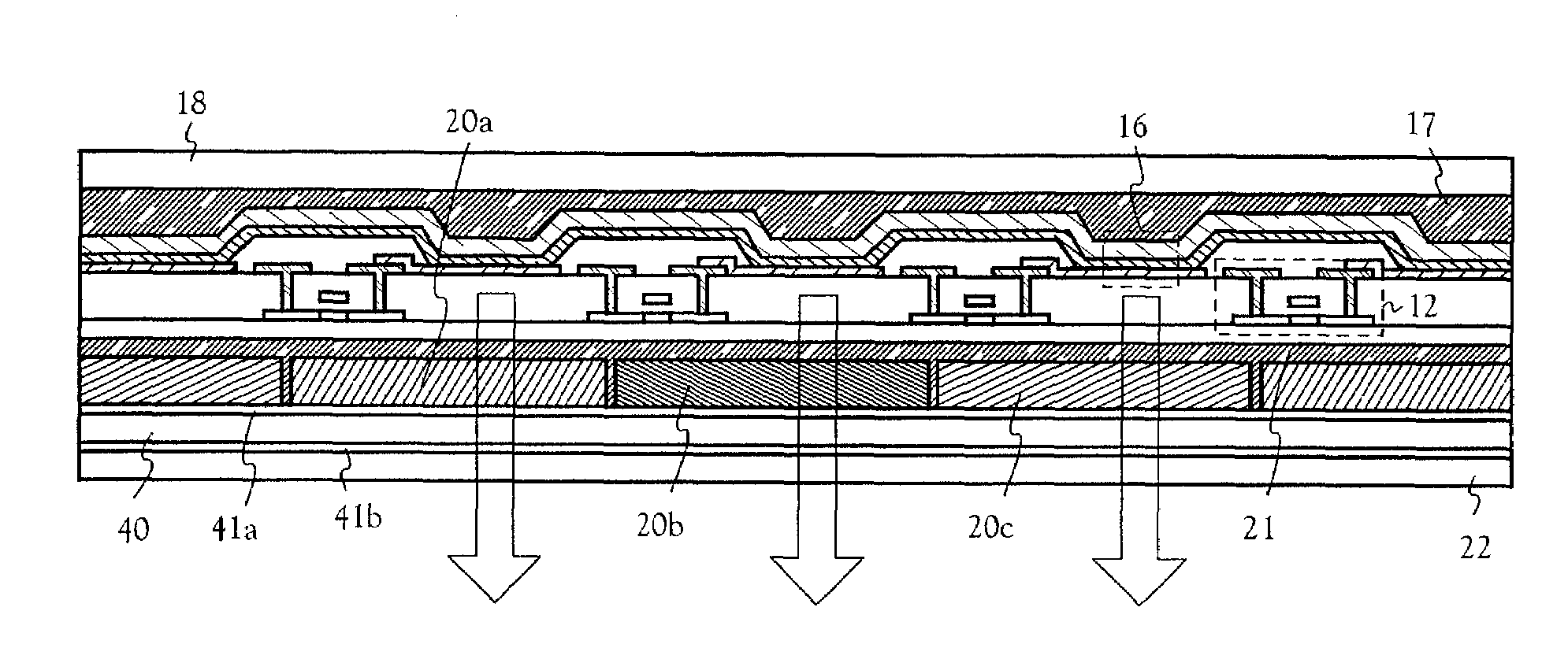
[0067]In this embodiment, a description will be made of an example of a light emitting device shown in FIGS. 1A and 1B or FIGS. 2A and 2B, in which a plastic film (a film formed of polymeric material) is used as a color filter substrate. A light emitting device of this embodiment is shown in FIGS. 4A and 4B. Note that reference numerals identical to those used in FIGS. 1A and 1B or FIGS. 2A and 2B may be referred to the descriptions of embodiment mode.

[0068]In FIG. 4A, a color filter film 40 is a film (plastic film) formed of a polymeric material, and protective films 41a and 41b are formed on both (front and back surfaces) surfaces thereof. Note that, in this embodiment, a plastic film is used, but a substrate made of hard plastic may be used.

[0069]Further, as protective films 41a and 41b, it is preferable that an insulating film is provided, which does not permeate water or oxygen or which hardly permeate water or oxygen. Typically, a carbon film, preferably a diamond like carbon ...


PUM


Abstract

An inexpensive light emitting device and inexpensive electric equipment are provided. A substrate on which a semiconductor element or a light emitting element is formed and a color filter are manufactured by separate manufacturing processes, and they are bonded to each other to complete the light emitting device. Thus, the yield of the light emitting device is improved and the manufacture period is shortened.

Description

BACKGROUND OF THE INVENTION[0001]1. Field of the Invention[0002]The present invention relates to a light emitting device having an element in which a light emitting material is interposed between electrodes, and to electric equipment in which the light emitting device is used in a display portion (a display or a display monitor). In particular, the present invention relates to a light emitting device using a light emitting material which provides electro luminescence (EL) (hereinafter referred to as EL material). Note that an organic electro luminescence display and an organic light emitting diode (OLED) are included in the light emitting device of the present invention.[0003]In addition, the light emitting material which can be used in the present invention includes all light emitting materials for producing light emission (phosphorescence and / or fluorescence) through singlet excitation, triplet excitation, or both excitations.[0004]2. Description of the Related Art[0005]Recently, ...

Claims


Application Information

Patent Timeline
Patent Type & Authority Patents(United States)
IPC IPC(8): H01L33/00H01L27/32H01L33/44
CPCH01L27/322H01L33/44H01L27/3281H01L27/3244H10K59/38H10K59/17H10K59/12
Inventor YAMAZAKI, SHUNPEIFUKUNAGA, TAKESHIKOYAMA, JUNINUKAI, KAZUTAKA
Owner SEMICON ENERGY LAB CO LTD
Why Eureka
Try Eureka