Thin layer element and associated fabrication process

a technology of layer elements and fabrication processes, applied in the field of thin layer elements, can solve the problems of agglomeration and disastrous for the continuation of the fabrication process, and achieve the effect of stabilizing the layer pattern

Active Publication Date: 2009-08-25
COMMISSARIAT A LENERGIE ATOMIQUE ET AUX ENERGIES ALTERNATIVES
View PDF21 Cites 0 Cited by
  • Summary
  • Abstract
  • Description
  • Claims
  • Application Information

AI Technical Summary

Benefits of technology

[0007]According to a first solution, the implantation is performed over at least a portion of the layer at the periphery of a support area of the pattern so as to modify the surface properties of the portion. This modifies the contact angles, which makes the pattern stronger. The presence of implanted species in the peripheral regions of the area of the layer that supports the pattern modifies the surface energies of the layer and / or of the interface between the pattern and the layer and therefore the contact angle at thermodynamic equilibrium. This contact angle is also known as Young's angle (referred to as the contact angle in the remainder of the document).
[0014]The invention also proposes a thin layer element including a layer of a first material that supports a pattern of a second material, characterized by a region doped with a chemical species over at least a portion of the layer-pattern assembly so as to stabilize the pattern on the layer.

Problems solved by technology

This kind of phenomenon, known as agglomeration, is disastrous for the continuation of the fabrication process.

Method used


Image

  • Thin layer element and associated fabrication process
  • Thin layer element and associated fabrication process
  • Thin layer element and associated fabrication process

Examples


second embodiment

[0051]Implantation of the pattern is not harmful in all cases, as explained in more detail below with reference to the FIG. 7 represents the profile of the concentration of atoms of arsenic (As) in the buried layer 2. The depth in the buried layer 2 relative to the upper surface of the buried layer 2 that is implanted is plotted on the abscissa. As in FIG. 6, the concentration of atoms of arsenic per cm3 is plotted on the ordinate.

[0052]If a 5 keV implantation energy is used (continuous line in FIG. 7), the typical depth of implantation is slightly less than 10 nm. Note that this typical depth is slightly greater than the depth of implantation obtained with the same energy in the nitride mask 6. In the case of a 10 keV energy (dashed line in FIG. 7), the depth of implantation is of the order of 15 nm.

[0053]When implantation is completed, there may follow an annealing step to ensure lateral diffusion of the implanted species into the buried layer 2. This results in doping of the per...

first embodiment

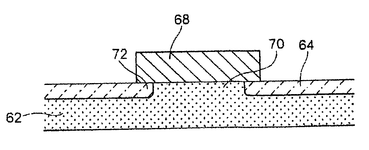
[0070]Due to the presence of these implanted regions 34, 36, as much on the surface of the buried layer 32 as within the thin layer pattern 38, the following two physical phenomena can work together to prevent dewetting of the thin pattern 38:[0071]modification of the surface energies of the buried layer 32 in the regions 34 thereof that do not carry the thin pattern 38, so as to modify the contact angles (in a similar manner to the effect produced in the first embodiment); and[0072]reduction of the speed of diffusion at the surface of the thin layer 38 by the doping of at least a significant portion 36 thereof.

[0073]The above two phenomena combine to keep the thin pattern in the form of a compact mass, especially if the thin layer element is heated to high temperatures, for example for cleaning by desorption. As is apparent, the combined application of the above two phenomena nevertheless implies that the doping of the thin pattern 38 does not cause problems in subsequent use of th...

third embodiment

[0074]In another embodiment, examples of which will be given below, implantation may be carried out before the layer-pattern structure is constituted. FIGS. 14 to 16 show the invention that uses this feature. In this embodiment, a layer 52 of silicon oxide (SiO2) undergoes implantation with a chemical species (for example arsenic) as shown diagrammatically in FIG. 14. After implantation, the layer therefore has the overall profile represented in FIG. 15, that is, a surface region 54 of the layer 52 that has undergone implantation and is therefore doped with the chemical species, while the buried regions of the layer 52 have not been significantly affected by the implantation.

[0075]The layer-pattern structure is then produced, for example, by forming the pattern 58 by a method analogous to that represented in FIGS. 1 and 2, or alternatively by individual or collective transfer of patterns onto the implanted surface, for example using molecular bonding. Due to the doping of the surfac...


PUM

PropertyMeasurementUnit
thicknessaaaaaaaaaa
depthaaaaaaaaaa
angle of incidenceaaaaaaaaaa

Abstract

A method is provided for fabricating a thin layer element, in which a layer of a first material supports a pattern of a second material having a thickness of less than 15 nm, including a step of doping by implanting a chemical species over at least a portion of the layer-pattern assembly to stabilize the pattern on the layer.

Description

RELATED APPLICATIONS[0001]This application claims priority from French Patent Application No. 0408989 filed Aug. 19, 2004, which is incorporated herein by reference.TECHNICAL FIELD[0002]The invention relates to a thin layer element and a process for fabricating this kind of element. In particular, the invention relates to a thin layer element for an electronic component.BACKGROUND[0003]In electronic component fabrication processes, elements are frequently used that consist of a layer made from a first material that supports a pattern made from a second material, for example in the form of a thin layer. This type of structure is seen in particular in the silicon-on-insulator (SOI) technology, as described in patent application FR 2 827 705 for the production of a transistor, for example. In this technique, a buried insulative material layer separates the pattern, which is part of the electronically active portion (for example a transistor), from the solid silicon substrate. During th...

Claims


Application Information

Patent Timeline
Patent Type & Authority Patents(United States)
IPC IPC(8): H01L21/00H01L21/265H01L21/762
CPCH01L21/26586
Inventor BARBE, JEAN-CHARLESVINET, MAUDFAYNOT, OLIVIER
Owner COMMISSARIAT A LENERGIE ATOMIQUE ET AUX ENERGIES ALTERNATIVES
Why Eureka
Try Eureka