Semiconductor laser diode for controlling width of carrier inner flow path
A technology of laser diodes and semiconductors, applied in the direction of semiconductor lasers, optical waveguide semiconductor structures, lasers, etc., can solve the problems of shortening the life of semiconductor laser diodes and decreasing the stability of semiconductor laser diodes, and achieve increased processing tolerance and reduced distortion , quick on/off switching effect
- Summary
- Abstract
- Description
- Claims
- Application Information
AI Technical Summary
Problems solved by technology
Method used
Image
Examples
no. 1 example
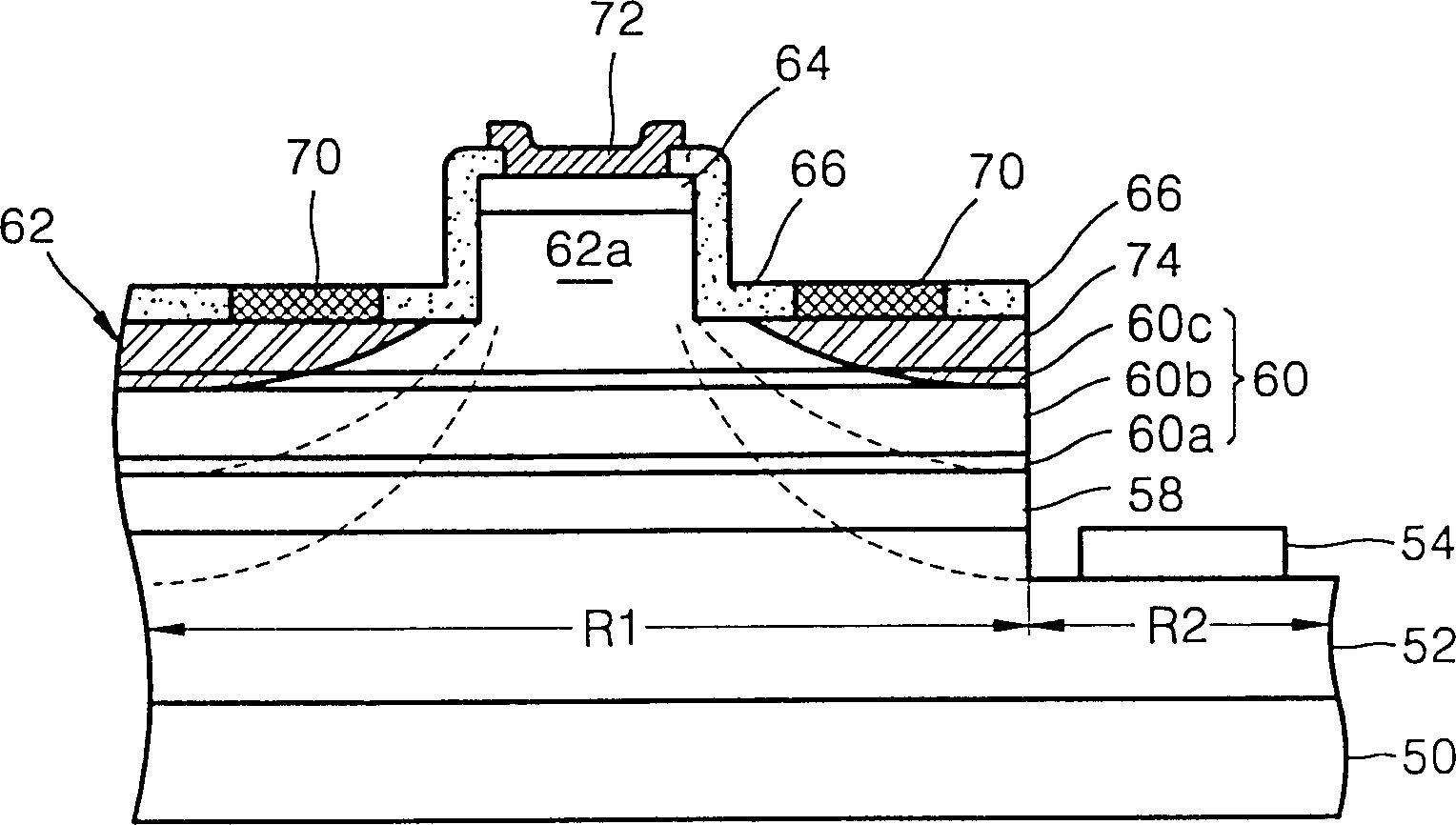
[0026] refer to image 3 , the first compound semiconductor layer 52 is formed on the substrate 50 . Preferably, the substrate 50 is grown on gallium nitride or a gallium nitride-based material. Therefore, the substrate 50 is preferably a sapphire substrate, a group III-V compound semiconductor substrate (for example, a GaN substrate), or a silicon carbide (SiC) substrate. The first compound semiconductor layer 52 which is a GaN-based III-V nitride semiconductor layer is formed of an n-type material or an undoped material. Preferably, the first compound semiconductor layer 52 is an n-GaN layer or a GaN layer. However, the first compound semiconductor layer 52 may be an AlGaN layer containing aluminum (Al) at a predetermined ratio or an InGaN layer containing indium (In) at a predetermined ratio. The first compound semiconductor layer 52 is divided into first and second regions R1 and R2. The first region R1 is wider and thicker than the second region R2. Therefore, a step ...
no. 2 example
[0044] The difference between the second embodiment and the first embodiment lies in the structure of the carrier inflow width controller. In the first embodiment, the ridge 62a is used as the second carrier inflow width controller. Therefore, in the first embodiment, there are first and second carrier inflow width controllers. However, in the second embodiment, there is only one carrier inflow width controller.
[0045] Specifically, as Figure 5 As shown in , the second cladding layer 62 and the second compound semiconductor layer 64 are sequentially formed on the resonance layer 60 . However, the second cladding layer 62 does not include the ridge 62a of the first embodiment, and the second compound semiconductor layer 64 is formed on the entire surface of the second cladding layer 62, not only on a part thereof. The second electrode 72 is formed on the second compound semiconductor layer 64 , and the carrier width controller 80 is symmetrically formed around the second ...
no. 3 example
[0048] In a third embodiment, a portion of the p-type electrode protrudes downward toward the active layer, and a carrier inflow width controller covered with an insulating layer surrounds the portion of the p-type electrode.
[0049] Specifically, see Figure 7 An n-type material layer 106 for generating laser light is formed on the first electrode 100 , having an n-type compound semiconductor layer 102 , an n-type cladding layer 104 and an n-type waveguide layer 108 a. The n-type waveguide layer 108a has a lower refractive index than the active layer 108b. A p-type material layer 113 for generating laser light having a p-type waveguide layer 108c, a p-type cladding layer 110c, and a p-type compound semiconductor layer 112 is formed on the active layer 108b. The p-type waveguide layer 108a has a smaller refractive index than the active layer 108b. The n-type waveguide layer 108 a of the n-type material layer 106 , the p-type waveguide layer 108 c of the p-type material laye...
PUM
 Abstract
Description
Claims
Application Information


