Imaging device package camera module and camera module producing method

a technology of camera module and camera module, which is applied in the direction of cross-talk/noise/interference reduction, television system, radio control device, etc., can solve the problems of underfill material flowing into the light receiving portion, adversely affecting development efficiency, and increasing the cost of manufacturing ceramic boards, so as to achieve the effect of improving the s/n ratio

Inactive Publication Date: 2009-09-01
KYOCERA CORP
View PDF14 Cites 25 Cited by
  • Summary
  • Abstract
  • Description
  • Claims
  • Application Information

AI Technical Summary

Benefits of technology

[0056]With the arrangement above, as the flip-chip packaging portion of each land of the bare-chip board of the semiconductor element is surrounded with the solid GND l...

Problems solved by technology

In the example shown in FIG. 24, though the underfill material is thus used for shielding the imaging device and increasing the adhering strength of the imaging device to the board, there is the possibility of causing the underfill material to flow into the light receiving portion.
A lens unit including the lens, the lens barrel and the holder in the above example is designed for exclusive use from time to time in order to meet the specification required and this may adversely affect development efficiency.
As the underfill material is prevented from flowing in by forming a projection on the ceramic board, there develops a problem arising from an increase in the cost of manufacturing ceramic boards.
Another conceivable method of preventing the underfill material from flowing in is to make the underfill material hard to flow by adding a solvent (filler) thereto as described above; however, the problem is that if the viscosity is thus raised, it will not only lower the workability but als...

Method used


Image

  • Imaging device package camera module and camera module producing method
  • Imaging device package camera module and camera module producing method
  • Imaging device package camera module and camera module producing method

Examples


first embodiment

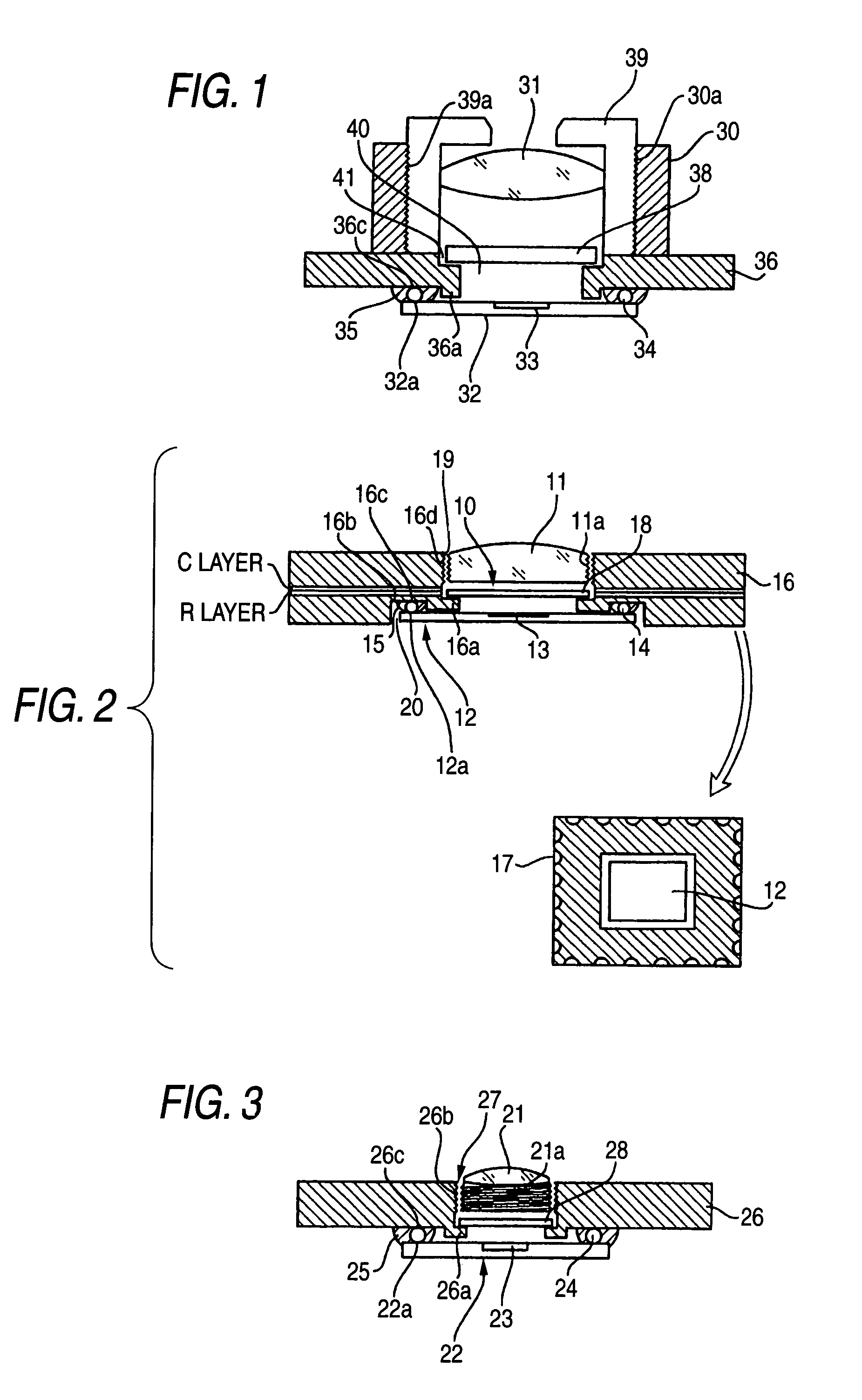
[0087]FIG. 1 is a block diagram showing a small-sized module camera as a first embodiment of the invention.

[0088]As shown in FIG. 1, an optical system is disposed on the top surface of a ceramic board and an imaging device is arranged on the undersurface thereof, for example, according to this embodiment of the invention.

[0089]Incidentally, HTCC (High Temperature Cofired Ceramics) or LTCC (Low Temperature Cofired Ceramics) is used for the ceramic board. HTCC is high temperature cofired ceramics and features a high dielectric coefficient. HTCC is inferior in working precision to the LTCC but less costly. LTCC is low temperature cofired ceramics and features low resistance and non-contractibility. LTCC is excellent in working precision and lower in dielectric coefficient than the HTCC (and is fit for a high-frequency circuit).

[0090]The LTCC OR HTCC (hereinafter called “LTCC”, to collectively represent both of them) 36 is employed for the board and black is adopted as a shielding color...

second embodiment

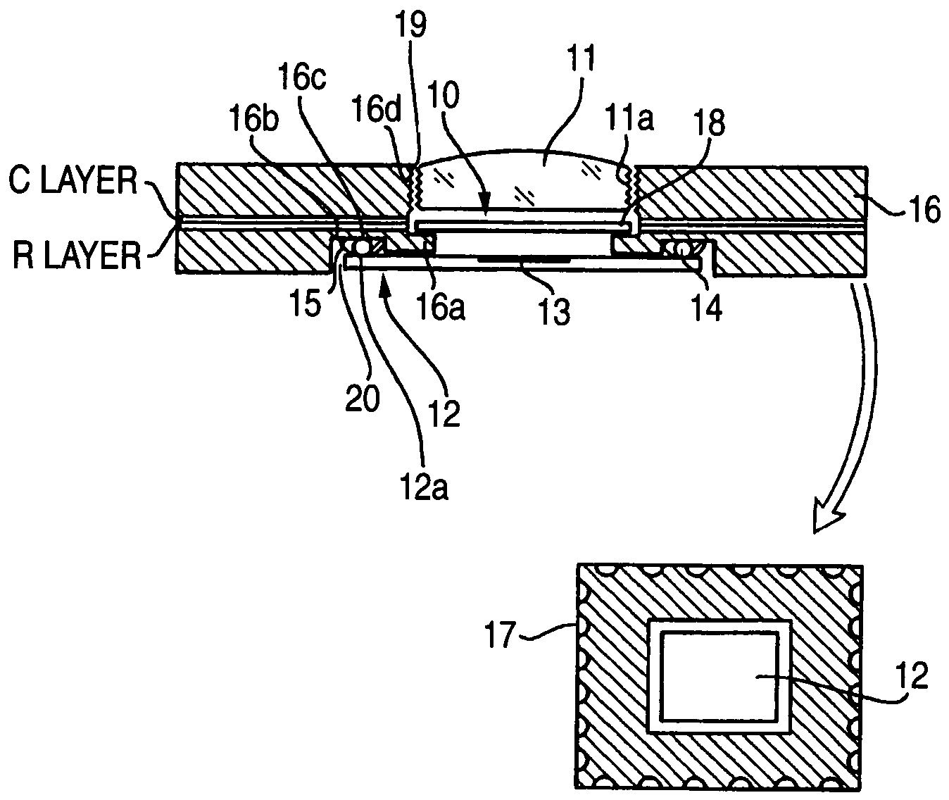
[0097]FIG. 2 is a block diagram showing a small-sized module camera as a second embodiment of the invention.

[0098]As shown in FIG. 2, an optical system and an imaging device are contained within a through-hole formed in a ceramic board, for example, according to this embodiment of the invention.

[0099]The LTCC or HTCC (hereinafter called the “LTCC” collectively representing both of them) 16 is employed for the board and black is adopted as a shielding color.

[0100]The LTCC 16 has a C and an R layer inside and electrically passive elements including capacitors and resistors, for example, are formable in these layers.

[0101]A through-hole 10 is provided in the LTCC 16 and the upper side of the through-hole 10 is in the form of a columnar hole, whereas the lower side thereof is in the form of a quadrangular hole. The columnar hole is equivalent to an optical-system containing portion 19 for containing an IR cut-filter 18 and a lens 11, and the quadrangular hole to an imaging-device contai...

third embodiment

[0108]FIG. 3 is a block diagram showing a small-sized module camera as a third embodiment of the invention.

[0109]As shown in FIG. 3, an optical system is contained in a ceramic board and an imaging device is provided on the undersurface of the ceramic board, for example, according to this embodiment of the invention.

[0110]LTCC 26 is used for the board as shown in FIG. 2.

[0111]A columnar through-hole is provided in the LTCC 26 and this through-hole is equivalent to an optical-system containing portion 27 for containing an IR cut-filter 28 and a lens 21. A thread portion 26b is formed on the inner wall of the optical-system containing portion 27. A support portion 26a for supporting the IR cut-filter 28 and preventing an underfill material 25 from flowing into the light receiving portion 23 of an imaging device 22 is formed in the boundary portion of optical-system containing portion 27 on the undersurface of the LTCC 26. The support portion 26a is projected from the undersurface of t...


PUM


Abstract

An IR cut-filter is fitted into a support portion within the optical-system containing portion of a ceramic board and a lens 11 is mounted in the ceramic board by screwing the lens.
In an imaging-device containing portion, an imaging device with a light receiving portion arranged therein is mounted outside the support portion by flip-chip packaging. Further, the vicinity of the flip-chip packaging portion is sealed with resin.
Additionally, on the base of the imaging-device containing portion of a ceramic package, the lands of an imaging device are so positioned as to correspond to the respective land positions of a ceramic package and patterns are electrically connected by melting a gold bump, whereby the imaging device is mounted by bare-chip packaging. The land portion is filled with an underfill agent and then sheet glass is mounted on a through-hole 5b and sealed with a sealing agent, so that the through-hole 5b for containing a light receiving portion is sealed up.

Description

BACKGROUND OF THE INVENTION[0001]The present invention relates to an imaging device package for use in a portable communication apparatus such as a mobile telephone, a portable information terminal such as a PDA, a digital camera and so forth, to a camera module and a camera using such a package and to a camera module producing method.[0002]The present invention relates to a structure in which a bare semiconductor chip board such as a CCD imaging device is mounted on a circuit board as well.[0003]Camera modules contained in mobile telephones such as portable telephones are required to be small-sized. It has so far been studied to mainly reduce the size in the x-y (plane) direction. With portable telephones being increasingly multi-functioned, however, camera blocks must be reduced in size and thickness as liquid crystal display units are replaced with EL elements.[0004]JP-A-2001-128072 discloses a camera module wherein improvement has been embodied in its thickness.[0005]FIG. 24 is ...

Claims


Application Information

Patent Timeline
IPC IPC(8): H04N5/225H01L31/0203H01L31/0232H05K1/02H05K3/32
CPCH01L27/14618H01L27/14625H01L31/0203H01L31/0232H04N5/2253H05K1/0219H04N5/2254H05K2201/10977H05K3/323H05K2201/09809H05K2201/10719H01L2224/29035H01L2224/17051H01L2224/29011H01L2224/73204H01L2224/81191H01L2224/14135H01L2224/05573H01L2224/05568H01L2924/00014H01L31/02325H04N23/54H04N23/57H04N23/55H01L2924/00012H01L2224/05599H01L27/146H04N25/00
Inventor AIZAWA, MITSUAKIITOH, HIROKINAKAI, MASANOBU
Owner KYOCERA CORP
Why Eureka
Try Eureka